
What is a PCB Ground Plane?
The ground plane is a fundamental element in PCB design, acting as a backbone that supports electronic circuits. A PCB ground plane is a large area of copper that serves as a common electrical reference point for all components on the board. It helps in maintaining a consistent voltage level across the PCB, providing a path for return currents and shielding against noise.
Types of PCB Ground Planes
Different types of ground planes cater to various design needs and complexity levels. Here’s an overview of the most common types:
Single-Layer Ground Plane
Single-layer ground planes are found on one side of the PCB, typically used in simpler or low-cost designs. While they provide basic grounding, they may fall short in handling high-frequency signals or complex routing requirements.
Two-Layer Ground Plane
Two-layer ground planes involve a separate layer dedicated to grounding, sandwiched between two signal layers. This setup offers better EMI shielding and signal integrity compared to single-layer designs, making it suitable for moderately complex circuits.
Multi-Layer Ground Plane
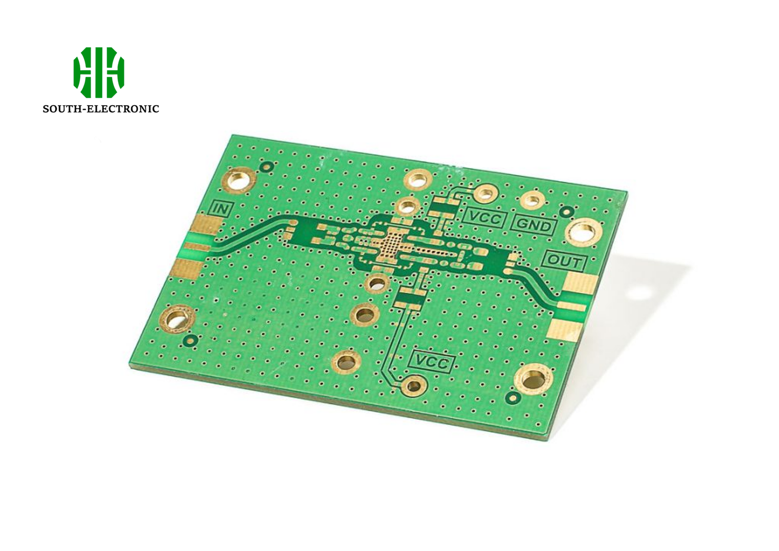
In multi-layer PCBs, ground planes are included in multiple layers, providing the best performance in terms of EMI reduction, signal integrity, and routing flexibility. These are essential in high-density and high-speed circuit designs.
| Type | Description | Pros | Cons |
|---|---|---|---|
| Single-Layer | One-sided ground plane | Cost-effective, simple | Limited EMI protection, less effective for high-frequency signals |
| Two-Layer | Ground plane between two signal layers | Better EMI protection, improved signal integrity | More complex and expensive |
| Multi-Layer | Multiple ground planes in a stacked configuration | Superior EMI shielding, excellent signal integrity, flexible routing | Highest cost, complex manufacturing |

Benefits of PCB Ground Planes
- Signal Integrity:A well-designed ground plane ensures a low-impedance path for return currents, which is crucial for maintaining signal integrity. It minimizes noise and prevents signal degradation, essential for reliable circuit performance.
- Electromagnetic Interference (EMI) Management:Ground planes act as shields against electromagnetic interference, absorbing and dissipating stray electromagnetic fields. This reduces crosstalk between traces and enhances the electromagnetic compatibility (EMC) of the PCB.
- Thermal Management:Ground planes also play a role in heat dissipation, especially important in high-power applications. They spread the heat generated by components more evenly across the PCB, reducing hotspots and enhancing the longevity of the board.
- Routing Flexibility:With ground planes, designers have more routing options, allowing for compact and efficient PCB layouts. This flexibility is particularly valuable in multi-layer designs where space is at a premium.
Best Practices for Implementing Ground Planes in PCB Design
Here’s a guide to some of these practices:
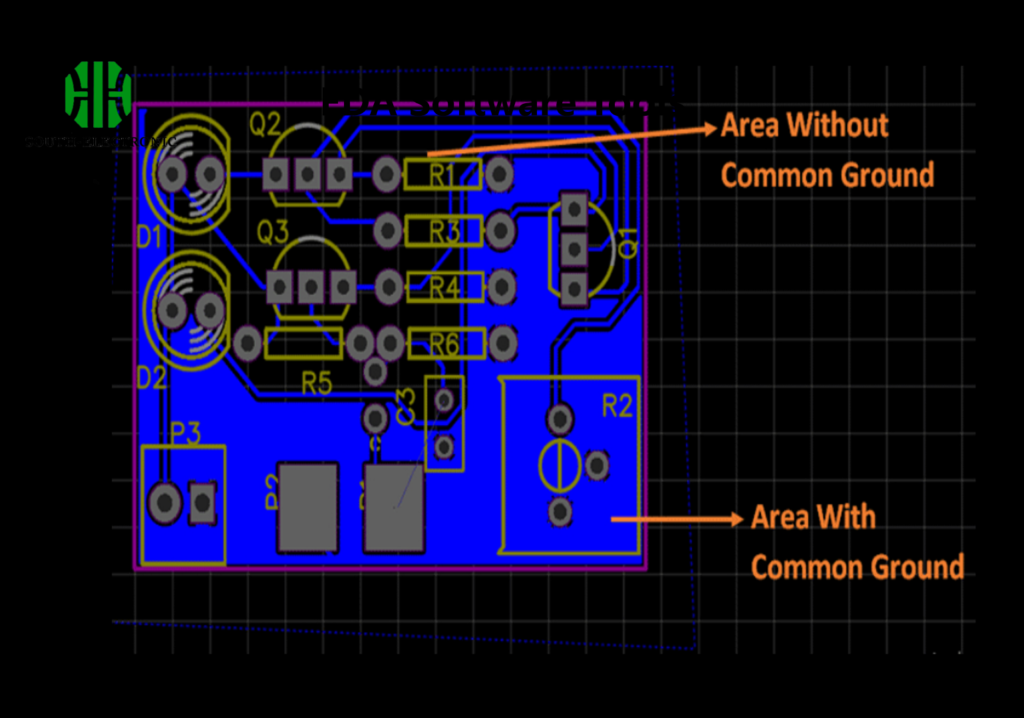
- Placement Considerations:Proper placement of the ground plane is crucial. It should be close to the signal traces and components to minimize loop area and inductance, enhancing signal integrity and EMI performance.
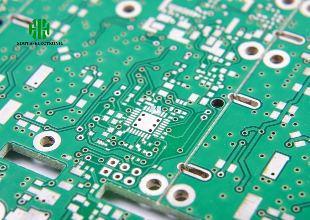
- Routing Techniques:When routing signal traces, they should be kept on the same layer as the ground plane whenever possible. This helps maintain a consistent impedance and reduces the risk of signal reflections. Avoiding sharp bends and maintaining adequate trace width are also important for signal quality.
- Connecting Ground Planes:For multi-layer PCBs, connecting ground planes through vias ensures a continuous ground path. Stitching vias, placed at regular intervals, help to maintain low impedance and minimize potential ground loops.
- Clearance and Spacing Rules:Adequate spacing between ground planes and other traces or components is necessary to prevent electrical shorts and ensure insulation. Following industry-standard clearance rules is vital for the reliability and safety of the PCB.
- Integrating Power Planes:Combining ground planes with power planes can further enhance a PCB’s performance. This setup allows for better power distribution and reduces noise coupling between power and signal lines.
- Case Studies and Real-World Examples:Including real-world examples of successful PCB designs using advanced ground plane techniques can provide practical insights and inspire innovative solutions.
If you’re a PCB designer, you need to know how to use ground planes. It’s a big part of being good at electronics. If you want your boards to work right and last a long time, you need to know how to use ground planes.

