

PCB testing nightmares draining your budget? Faulty boards slipping through cracks? Simple solutions exist right on your design canvas. Discover hidden testing assets you already own.
Common low-cost PCB test points[^1] include bare copper pads[^2], uncovered vias, and through-hole component legs[^3]. These options minimize extra materials since they use existing board features like SMT component pads or drilled holes. They reduce prototyping costs significantly for hobbyists and startups.

Now that we’ve cracked the types puzzle, let’s explore smart ways to design these budget-friendly solutions right into your board. There’s more cost-cutting wisdom ahead.
How to design low-cost PCB test points?
Design chaos doubling your expenses? Unnecessary custom features inflating bills? Transform ordinary components into test access hubs through clever placement tactics.
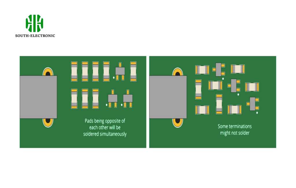
Place exposed copper pads near key circuits and convert through-hole component legs into probe targets[^4]. Ensure pads are 0.8mm minimum diameter with zero solder mask coverage. Align all test pads on grid for automated probing compatibility during low cost pcb manufacturing.
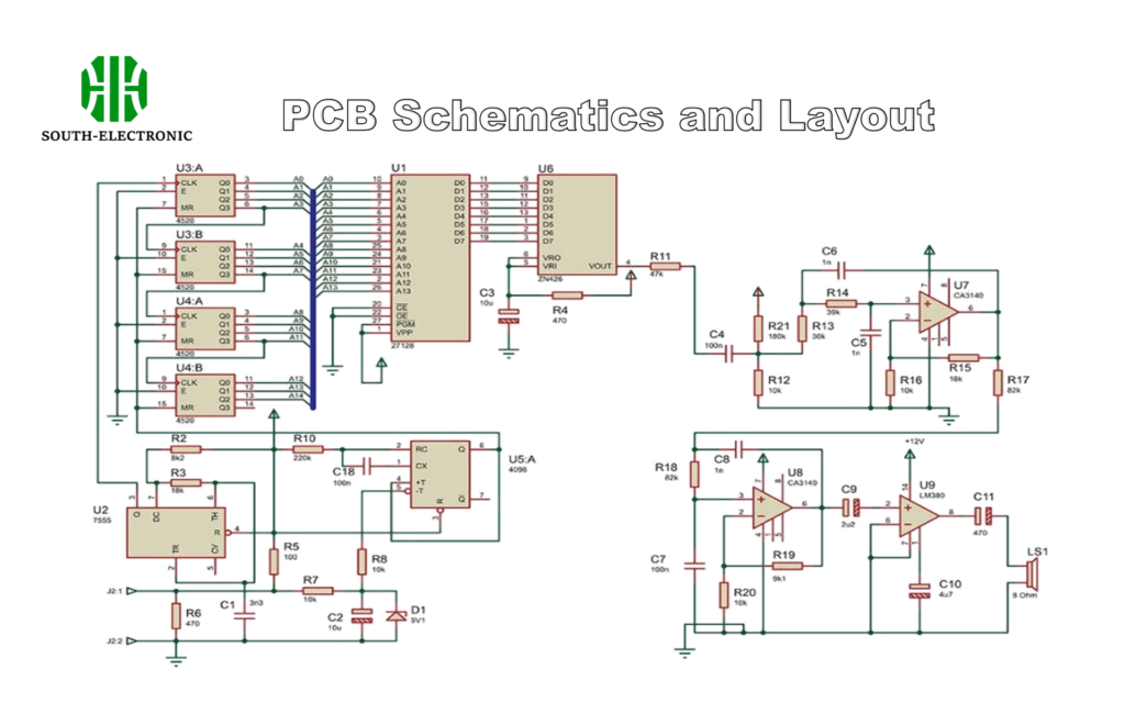
Intelligent Test Point Design Principles
Smart test placement follows critical logic chains. We strategically leverage existing structures and minimize specialized additions. Below table contrasts effective approaches:
| Tactics | Implementation | Cost Saving Impact |
|---|---|---|
| Pad Reuse | SMT component landing pads | 100% material saving |
| Bare Vias | Remove solder mask from plated holes | No additional drilling |
| Component Adaptation | Probe contact on resistor/capacitor legs | Eliminates dedicated points |
Repurposing through-hole components delivers strongest savings. I position resistors perpendicular to test probe paths allowing direct access to leads. Each reused via cuts $0.02-$0.05 per test point in low cost pcb prototype runs. Maintaining 1.5mm clearance between probe targets prevents accidental shorts during testing. Aligned layouts also speed up assembly verification for low cost pcb assembly services.
Are Low-Cost PCB Test Points Reliable?
Questioning probe point durability? Data glitches ruining measurements? Price doesn’t dictate performance when physics-backed rules govern reliability.
Properly implemented low-cost test points match expensive alternatives in functionality. Meeting plating thickness standards (25μm minimum) prevents wear issues. Surface oxidation gets controlled with regular low volume cleaning cycles during checks.
The Steel-Core Truth About Durability
Electrical stability comes from physical fundamentals, not price tags. Let’s unpack key reliability pillars:
| Risk Factor | Simple Test Points | Mitigation Approach |
|---|---|---|
| Surface Oxidation | Bare copper exposure | Annual contact cleaning |
| Mechanical Stress | Thin pad anchoring | Octagonal pad shapes distribute force |
| Signal Integrity | Shared ground paths | Dedicated return vias in test clusters |
Through-hole leads offer inherent stability – steel-reinforced legs withstand hundreds of probe contacts. One US maker documented 7,300+ probe cycles on capacitor legs. For humidity-prone areas, I specify ENIG plating on pads for extra oxidation resistance when ordering low cost pcb usa batches. Consistent data reads demand isolation from noisy circuits – maintain 3X trace width clearance.
Where to Source Dirt-Cheap PCB Test Points in Bulk?
Vendor hunting wasting engineering hours? Bulk pricing tricks inflating costs? Direct supplier partnerships unlock volume discounts without quality sacrifice.
Order integrated test pads[^5] as PCB design elements from Proto-Electronics or PCBWay. Eliminate separate parts buying by including vias/pads in board files themselves. This leverages manufacturers’ economies of scale when placing low cost pcb assembly orders.
Bulk Acquisition Master Plan
Strategic sourcing combines physical suppliers with digital platforms. Analyze these bulk channels:
| Source Type | Key Providers | Best For |
|---|---|---|
| Board Features | JLCPCB, OSH Park | Prototype/test pad integration |
| Standalone Points | DigiKey, Mouser | Repair/replacement units |
| Surplus Channels | eBay, Electronic Goldmine | Sub-$0.01 point liquidation |
Domestic supplier Macrofab excels for urgent USA needs – 3-day turnkey assembly includes test feature integration. For 500+ unit batches, Shenzhen factories halve your expenses. Always request HAAS (high-availability automated sourcing[^6]) pricing tiers and verify lead times in writing. Remember: test points embedded in fabrications hold better during low cost pcb manufacturing than retrofit solutions.
Conclusion
Simple exposed pads and vias slash testing budgets effectively when designed right. Properly implemented, they deliver professional reliability at hobbyist costs across prototyping and bulk production phases.
[^1]: Explore this link to understand how low-cost PCB test points can significantly reduce your prototyping costs.
[^2]: Learn about the role of bare copper pads in PCB testing and their benefits for cost-effective designs.
[^3]: Discover how through-hole component legs can enhance your PCB testing strategy and save costs.
[^4]: Find out how probe targets are utilized in PCB design to improve testing efficiency and reliability.
[^5]: Find out how integrated test pads can streamline your PCB design process and reduce costs.
[^6]: Learn about high-availability automated sourcing and how it can optimize your PCB manufacturing process.

