

When reviewing user design drawings, we often find that the pad size is too large or too small. So what are the design standards and what impact will it have on production?
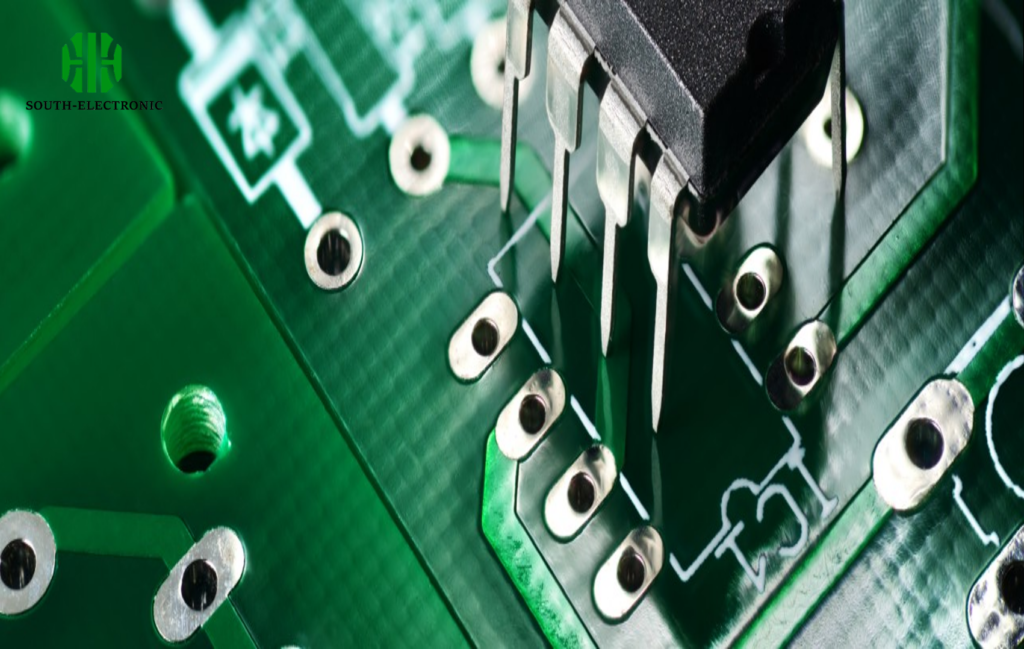
When arranging PCB components, designers should consider the difference in the minimum spacing between components relative to the thickness of the components. Generally, the spacing should be increased between larger electronic components to avoid adding thin components, but this will eventually cause welding defects. Secondly, the components are soldered to the PCB through the leads on the PCB, and the printed wires connect the pads to achieve the electrical connection of the components in the circuit. During the welding process, if people do not understand this aspect, it is easy to damage the pads on the PCB, which will seriously cause the entire circuit board to be scrapped.
There are also corresponding standards for the size and design of PCB pads.
-
The minimum single side of all pads is not less than 0.25mm.
-
The maximum diameter of the entire pad does not exceed 3 times the component aperture.
-
In the case of dense wiring, it is recommended to use oval and rectangular connection plates.
-
The diameter or minimum width of the pad of a single-sided board is 1.6mm; the weak current circuit pad of a double-sided circuit board only needs to increase the aperture by 0.5mm. If the pad is too large, it is easy to cause unnecessary continuous welding.
-
Pads with an aperture greater than 1.2mm or a diameter greater than 3.0mm should be designed as diamond or plum blossom-shaped pads.
-
All machine-inserted components need to be designed as drip pads in the direction of the bent legs to ensure that the solder joints at the bent legs are complete.
-
The pads on large areas of copper skin should be chrysanthemum-shaped pads, and there should be no virtual welding.

Pay special attention to manual soldering on PCBs. Remember not to use very high temperature soldering irons or tin furnaces to operate the pads, as this can easily cause the pads to fall off and cannot be remedied.
Unreasonable pad design directly affects the connection reliability between components and circuit boards. Improper design may cause inaccurate component soldering positions, affecting the electrical and mechanical properties of the circuit. At the same time, it increases the incidence of failures, reduces assembly speed, and increases repair costs. Reasonable pad design can reduce rework and repair during welding and improve production efficiency.
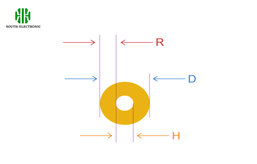
Jiepair has standard production requirements for pad apertures, and users can adjust the design parameters according to the requirements:
①Double-sided board: 0.2mm (inner diameter)/0.5mm (outer diameter)
②Multilayer board: 0.15mm (inner diameter)/0.25mm (outer diameter)
-
The outer diameter must be 0.1mm larger than the inner diameter, and it is recommended to be larger than 0.15mm
-
The minimum hole is recommended to be 0.2mm or more
In summary, PCB pad design has many effects on production. Reasonable pad design can not only improve product reliability and quality, but also improve production efficiency and reduce costs. Therefore, designers must understand the design of pads and their applications more carefully.

