
Impedance issues ruin PCB performance. Signals distort, devices malfunction. I discovered three impedance types solve these nightmares. Learn them to upgrade your designs.
Resistive impedance[^1] comes from resistors, reactive impedance from capacitors/inductors, and complex impedance mixes both. Understanding these prevents signal loss in controlled impedance PCBs.
These three types form the foundation of modern electronics. Stick with me to explore deeper concepts like controlled impedance traces and why they matter for high-speed designs.
What Exactly is Controlled Impedance and Why Does It Matter So Much in PCBs?
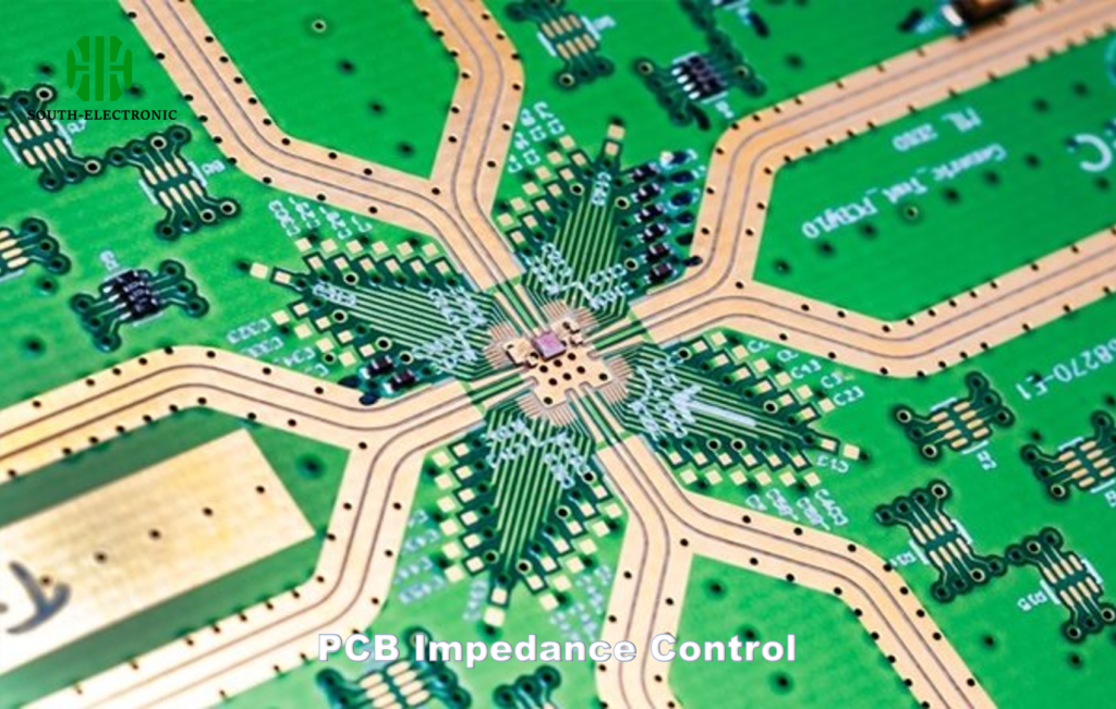
Chaotic signals crash PCB systems. Errors multiply, devices fail. Controlled impedance[^2] saves your circuits. I use it daily for reliable high-speed boards.
Controlled impedance maintains consistent electrical resistance in traces. It matters because mismatches cause signal reflections that corrupt data. This is critical for PCBs handling high-frequency signals.

Why Impedance Control Prevents Failures
All signals face opposition when traveling through copper traces. This opposition is characteristic impedance. When mismatched, energy bounces back like echoes in a tunnel. These reflections cause three major issues:
- Data errors in digital signals
- Reduced power in RF circuits
- Timing delays across systems
| Problem | Without Control | With Control |
|---|---|---|
| Signal Integrity | Distorted waveforms | Clean transitions |
| Data Transfer | Packet losses | Error-free transmission |
| Frequency Limits | < 1 GHz | 5+ GHz applications |
I specify controlled impedance traces when designing DDR memory interfaces. This ensures accurate clock timing. Without it, even advanced processors behave unpredictably. Modern impedance calculators help achieve precision matching while avoiding costly post-production fixes.
What is the difference between controlled dielectric and controlled impedance?
Designers confuse these terms constantly. Projects face delays, budgets blow up. Clarity prevents these headaches in your PCB process.
Controlled dielectric[^3] manages material properties like Dk value. Controlled impedance focuses on trace dimensions. They work together; dielectric stability affects impedance accuracy.

How Materials and Measurements Interact
Controlled dielectric forms the foundation. It ensures the insulation between copper layers maintains consistent electrical properties. This dielectric constant directly impacts impedance along controlled impedance traces. Consider these relationships:
| Factor | Controlled Dielectric Role | Controlled Impedance Focus |
|---|---|---|
| PCB Layer | Uniform material thickness | Trace width/space tuning |
| Key Metric | Dielectric constant[^4] (Dk) | Target impedance value |
| Validation | Material certification | Impedance testing |
Your PCB stackup needs both elements working together. For example, my RF designs require specific Er values to achieve impedance targets. This becomes critical when using impedance tables to map out microstrip configurations. Always verify both specifications on your fabrication drawings. Production variations in either area will degrade high-frequency performance.
How to test controlled impedance in PCBs?
Testing failures waste time and money. Debugging becomes impossible. These proven methods guarantee your controlled impedance traces meet specifications.
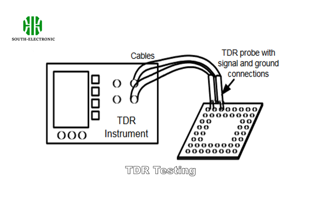
Use Time Domain Reflectometry[^5] (TDR) equipment testing. It send pulses along traces to measure reflections, showing impedance value variations throughout the signal path.
Step-by-Step Testing Methodology
Accurate verification involves both measurement tools and reference standards. Here's how I validate impedance in production:
-
TDR Setup
Connect equipment to test coupons designed alongside your PCB. This gives consistent access points. Modern TDR equipment provides precise waveform analysis showing deviations. -
Cross-Section Sampling
Confirm physical trace dimensions match designs. Any variation in width or dielectric spacing alters results. This catches manufacturing defects early. -
Reference Standards
Compare against a controlled impedance table for expected values. This baseline helps interpret TDR readouts correctly.
| Test Method | Accuracy Range | PCB Stage |
|---|---|---|
| TDR | ±3% Ω | Final boards |
| Coupon Testing | ±5% Ω | Production validation |
| Impedance Calculator | ±10% Ω | Design phase |
Simulate designs before manufacturing using controlled impedance calculators. I frequently employ these tools to predict results for complex stackups. Physical testing remains essential though. Always analyze multiple board samples across the panel since material inconsistencies occur.
Conclusion
Mastering impedance types solves signal issues. Use controlled impedance techniques to ensure reliable PCBs. Now go build better boards.
[^1]: Learn about resistive impedance to understand its role in maintaining signal quality in electronic circuits.
[^2]: Understanding controlled impedance is crucial for ensuring signal integrity in high-speed PCB designs.
[^3]: Learn about controlled dielectric to ensure material properties support impedance accuracy in your designs.
[^4]: Understanding the dielectric constant is essential for achieving desired impedance levels in PCB designs.
[^5]: Explore TDR as a method for accurately measuring impedance and ensuring PCB reliability.

