
Ever had a gadget break because weak solder joints failed? That’s frustrating! Through-hole components solve this by anchoring parts securely. They prevent loose connections in rough conditions.
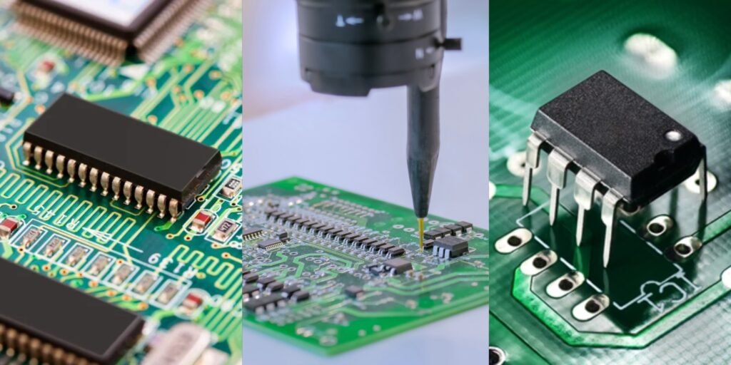
Through-hole components feature leads inserted into PCB holes and soldered. They create strong mechanical bonds and reliable electrical pathways. This durability suits high-stress applications like industrial machinery or automotive systems better than surface-mount parts.

Now that we understand their role, let’s explore key aspects of this technology. I’ll cover essential technical details in the next sections.
What’s a Through-Hole Via (PTH vs. NPTH)?
Designing PCBs involves confusing terminology. Wrong via choices cause connection failures! Let me simplify plated and non-plated holes.
PTH vias have metal plating inside holes for electrical connections. NPTH vias are empty holes for mechanical mounting. PTH carries signals between layers while NPTH accommodates screws.
Understanding Via Functions
Vias connect copper layers in a through hole pcb[^1]. Their type impacts performance:
| Via Type | Metal Lining? | Electrical Use? | Common Applications |
|---|---|---|---|
| PTH | Yes | Yes | Component leads, trace routing |
| NPTH | No | No | Mounting points, heat dissipation |
PTH carries signals vertically through the board. CPU sockets often rely on them. NPTH supports physical assembly without electricity. For example, chassis screws need NPTH. Mixing these creates problems! Verify your design specs before prototyping.
What Are the Key Differences Between Through-Hole and Surface Mount (SMT) Technology?
Choosing board assembly methods feels overwhelming. Wrong picks escalate costs! Compare surface mount vs through hole approaches clearly.
Through-hole parts insert leads into holes. SMT components sit directly on pads. Manual repairs suit through hole better, while SMT enables miniaturization. Heat resistance differs too.

Deciding Your Assembly Method
Critical factors determine the right choice:
| Factor | Through-Hole | SMT |
|---|---|---|
| Strength | Superior mechanical bonds | Vulnerable to vibration |
| Size | Bulky; limits PCB density | Enables compact designs |
| Assembly Cost | Higher labor due to drilling | Automated placement cheaper |
| Repairability | Simple solder replacement | Requires specialized tools |
Prototyping favors thru hole for hand-soldering ease. Mass production leans toward SMT for speed. Your project’s environment determines priority. Cars need durability; phones need small size.
What Specific Rules Do I Need to Consider When Designing a PCB for Through-Hole Assembly?
Missed design rules ruin PCB functionality! Avoid manufacturing rejects with planning.
Maintain 100mil clearance around hole pads. Avoid routing traces near NPTH sites. Use teardrop pads for stress reduction. Verify hole/pad diameter ratios first.

Design Checklist for Reliability
Optimize through hole pcb reliability:
-
Pad dimensions
- Outer pad diameter = drill size + 20 mils
- Inner layers need 30mil larger pads
-
Thermal relief
- Connect pads to planes with 4 copper spokes
- Prevents solder wicking during reflow
-
Drill alignment
- Place holes 0.5mm from board edges minimum
- Prevent breakout during fabrication
-
Footprint accuracy
- Match CAD models to datasheet dimensions
- Account for lead bend radii
Test designs with 3D prototypes when possible. Adjust tolerances for aged drill bits.
What Are the Size Limitations (Drill Hole, Pad Sizes) for Reliable THT Assembly?
Component sizing mistakes crack solder joints! Prevent field failures with precision standards.
Standard drill holes range from 0.3mm to 1.3mm. Pads should exceed hole diameter by 0.6mm. Axial part leads need 0.8mm+ annular rings.
Key Dimension Guidelines
Follow these smt vs through hole[^2] size rules:
| Component Type | Minimum Hole Size | Recommended Pad Size | Risk of Violation |
|---|---|---|---|
| Resistors/Capacitors | 0.4mm | Hole size + 0.8mm | Solder fractures |
| Connectors | 0.8mm | Hole size + 1.2mm | Poor pin contact |
| Transformers | 1.0mm | Hole size + 1.5mm | Mechanical instability |
Smaller holes increase drilling costs. Oversized pads reduce routing space. Balance these during through hole components[^3] placement. Verify with assembly partners before finalizing.
Conclusion
Through-hole technology provides essential durability for demanding electronics. Proper through hole pcb design ensures reliable performance. Choose it when strength matters most.
[^1]: Explore this resource to understand the benefits and applications of through hole PCBs in electronics design.
[^2]: This link will clarify the key differences between SMT and through hole technology, helping you make informed design choices.
[^3]: Learn about through hole components and their applications to enhance your understanding of PCB assembly techniques.

