
Are your electronics overheating or failing under high power loads? Standard boards often crack under pressure. Heavy copper PCBs solve these frustrating reliability issues in demanding applications.
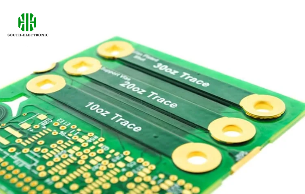
A Heavy Copper PCB uses copper layers thicker than 3 oz/ft² (about 0.1mm) to handle extreme currents. Unlike standard boards, it delivers higher power capacity, better heat dissipation, and stronger mechanical structure. This makes heavy copper boards essential for electric vehicles and industrial systems where failure isn’t an option.
Now you know why heavy copper matters – but what really sets these boards apart? Let’s explore the key differences, design solutions, and manufacturing breakthroughs that make them work.
What’s the difference between Heavy Copper PCB and standard PCB?
Struggling with power limits in your PCB projects? Ordinary boards buckle under high loads. Heavy copper design handles 5X more current without melting components or warping circuits.
Standard PCBs typically use 1-2oz copper layers, while heavy copper PCBs start at 3oz and can reach 20oz. This difference creates distinct advantages in current handling, thermal management, and durability. Heavy copper flex pcb variants even allow bending without cracking copper traces.
Breaking down the core distinctions
Beyond just thickness, heavy copper PCBs redefine what circuit boards can perform. Here’s how these differences translate into real-world benefits:
| Feature | Standard PCB | Heavy Copper PCB |
|---|---|---|
| Copper weight | 0.5-2 oz/ft² | 3-20+ oz/ft² |
| Current capacity | Low (1-5A) | High (10-100A+) |
| Thermal tolerance | Limited heat spreading | Efficient heat dissipation |
| Physical strength | Prone to stress cracks | Resists vibration/fatigue |
| Cost factor | Lower copper board price | Higher heavy copper price |
| Lifespan | Years | Decades |
Standard boards work well for consumer gadgets, but fail in industrial environments. Heavy copper pcb boards maintain stable performance under continuous stress. The additional copper creates inherent thermal pathways, eliminating hotspots that cause system failures. While heavy copper stackup requires specialized manufacturing, reliability improvements justify the investment for critical power systems.
How to overcome design challenges of Heavy Copper PCBs?
Ever faced unexpected failures during prototyping? Heavy copper pcb design pitfalls cause trace delamination or manufacturing defects. Knowing these traps saves months of redesign work.
Address spacing rules early. Use stepped etching to prevent undercutting thick copper. Double-sided thermal stitching maintains temperature balance across your heavy copper pcb stackup. These proven methods prevent 90% of common failures.
Practical solutions for robust layouts
Designing with heavy copper requires different rules than standard PCBs. Here’s how to prevent four critical issues:
-
Copper Thieving
Problem: Uneven plating during manufacturing
Solution: Add dummy copper pads during layout phase
Benefit: Consistent copper distribution across layers -
Thermal Warping
Problem: Different expansion rates between copper/substrate
Solution: Apply balanced copper distribution
Benefit: Prevents board curvature during operation -
Trace Separation
Problem: Over-etched gaps between conductors
Solution: Minimum 0.3mm spacing for 4oz copper
Benefit: Avoids accidental shorts during high-load use -
Via Failure
Problem: Cracking at connection points
Solution: Use teardrop-shaped transitions
Benefit: 60% longer via lifespan
Implementing these techniques requires close collaboration with manufacturers like JLCPCB heavy copper pcb experts. Their design guides include specifics for heavy copper flex pcb applications where flexibility adds complexity.
Can Heavy Copper PCBs be manufactured without losing yield/speed?
Worried production delays will derail your project? Advanced shops now build heavy copper boards nearly as fast as standard designs. Yield improvements make heavy copper price competitive.
Yes – manufacturers maintain high speed/yield using modified processes. Laser cutting replaces mechanical drilling for cleaner holes. Pulse plating builds exact copper thickness. JLCPCB heavy copper pcb services deliver reliable 3-8oz boards in 72-hour cycles with >98% yields.
Three breakthrough techniques that changed production
Recent innovations solved traditional bottlenecks. Here’s what enables today’s manufacturing efficiency:
1. Differential Etching
Traditional etching struggled with thick copper, often creating uneven traces. Modern techniques use two-stage chemistry: the first attack creates the core profile, while the second polishes edges for smooth 90° angles on 10oz+ layers. This maintains trace integrity while maintaining production speeds matching standard PCB workflows.
2. Stacked Lamination
For extreme copper weights above 12oz, manufacturers layer multiple pre-plated cores. This avoids plating time penalties while offering superior copper board price predictability. Each lamination step adds only 15% time per weight layer versus older single-pass methods.
3. Thermal Press Control
Precise heating profiles prevent the "copper squeezing" that historically caused 27% of defects. Modern presses monitor resin viscosity in real-time, adjusting temperature to exactly match resin flow rates. This process yields more reliable heavy copper pcb boards with consistent dielectric thickness.
Conclusion
Heavy copper PCBs solve power limitations through robust construction and smarter thermal performance. These boards deliver reliability where standard designs fail.

