
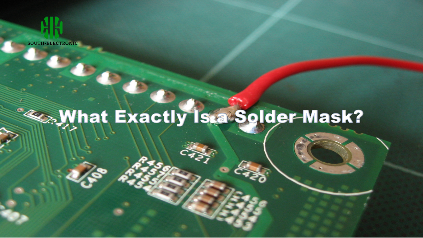
Ever ruined a circuit board with accidental solder bridges? Your frustration ends here.
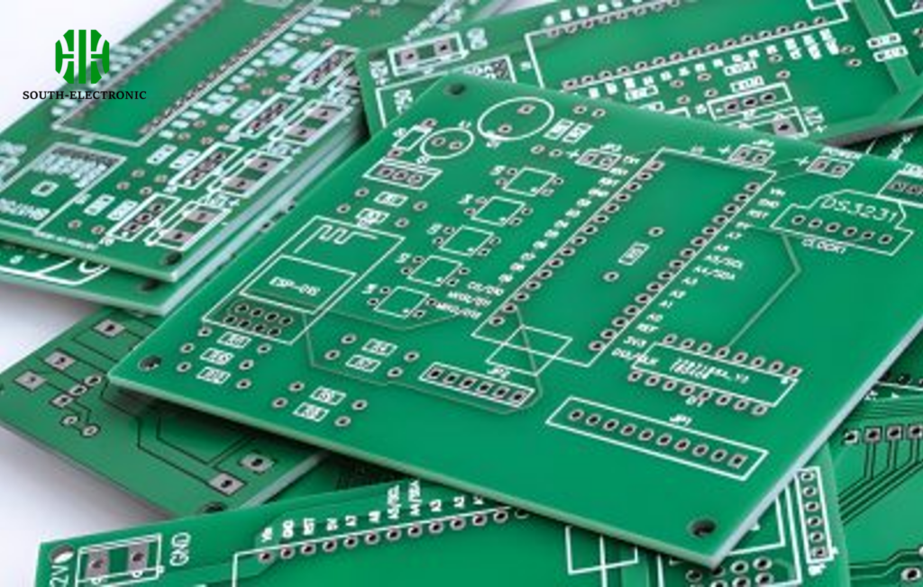
A solder mask is a protective polymer coating on PCBs that blocks solder from sticking to unnecessary copper traces. This prevents electrical shorts and shields against corrosion.

Understanding a circuit board solder mask is just the start. Let’s explore its key features.
What Colors Can a PCB Solder Mask Be?
Tired of boring green electronics? Your PCB doesn’t have to be dull.
Standard colors include green, red, blue, black, or white. Green dominates due to better inspection visibility and lower costs.
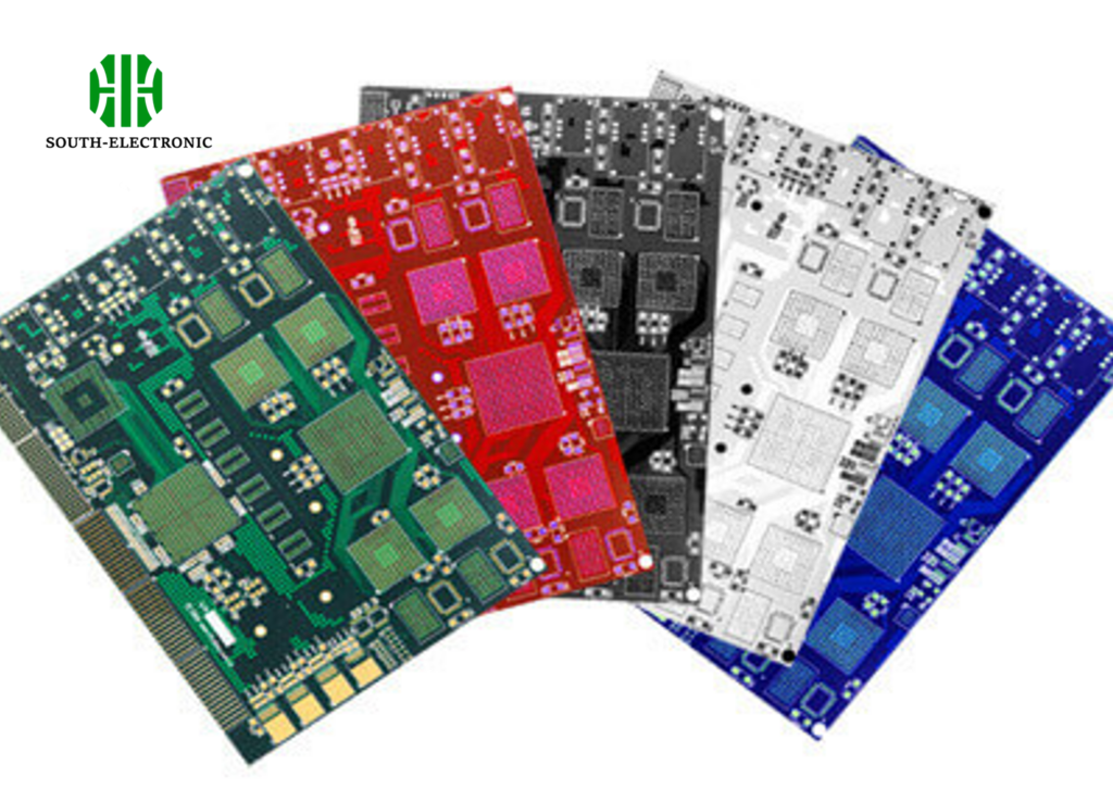
Why Color Matters
| Color | Primary Use | Visibility Rating (1-5) |
|---|---|---|
| Green | General electronics | ★★★★★ |
| Blue | Consumer gadgets | ★★★★☆ |
| Black | High-end devices | ★★★☆☆ |
| Red | Industrial controls | ★★★★☆ |
| White | LED/Light-sensitive boards | ★★☆☆☆ |
Green solder mask rules for practical reasons. It’s cheap and reveals manufacturing flaws easily under light. Red or blue work when branding matters but cost 10-20% more. Black looks sleek but hides defects. Avoid white solder mask unless needed – it turns yellow during heat curing. Color choice balances looks, cost, and inspection needs.
LPI vs. Dry Film Solder Mask: Which Type Is Best for Your PCB Project?
Struggling with uneven coating on complex boards? Your choice matters.
Liquid Photoimageable (LPI) offers high accuracy, while dry film suits dense boards. For hobbyists, LPI suffices.

Breaking Down the Differences
| Feature | LPI Solder Mask | Dry Film Solder Mask |
|---|---|---|
| Cost | $ $ | $$$$ |
| Use Case | Standard boards | HDI/microvias |
| Accuracy | 0.1mm lines | Under 0.05mm lines |
| Durability | Good | Excellent |
| DIY Friendly | Yes | No |
LPI applies like screen-printing ink using UV solder mask processes. It’s affordable for most projects but thinner. Dry film involves heat-laminated polymer sheets – perfect for phone motherboards yet costs triple. My failed drone project proved LPI’s limits: its 0.1mm gaps caused solder bridges on microscopic components. For complex layouts, dry film’s precision justifies its price.
How Is the Solder Mask Applied?
Worried about messy coatings ruining tiny pads? Master the process.
The UV solder mask process involves coating, masking, UV exposure, development, and curing. Automated machines ensure precision.
Step-by-Step Application
| Stage | Purpose | Critical Factor |
|---|---|---|
| Cleaning | Remove oxidation | Chemical purity |
| Coating | Apply epoxy layer | Uniform thickness |
| Exposure | Harden mask with UV light | Exposure time |
| Development | Remove unexposed areas | Chemical temperature |
| Curing | Final hardening | Heat duration |
After cleaning the copper, I like spraying LPI solder mask evenly. UV light hardens it while covered with a patterned film. Uncured parts dissolve in developer solution. Finally, baking locks it in. Bubbling happens if humidity exceeds 60% during coating. A 10°C developer solution change prevented my last factory defect. Consistent thickness decides quality – too thin invites corrosion.
Solder Mask Quality Standards:Peeling, Bubbling, or Poor Coverage?
Frustrated by flaking boards after assembly? Recognize red flags.
Top standards like IPC-SM-840 forbid peeling, bubbling, or poor coverage. Visual inspection finds 80% of defects.

Flaw Detection Guide
| Defect | Cause | Solution |
|---|---|---|
| Peeling | Contaminated copper | Clean with plasma tech |
| Bubbling | Moisture exposure | Control humidity |
| Poor coverage | Low viscosity mask | Adjust epoxy mix |
| Orange peel | Fast curing | Slow bake cycles |
| Solder skip | Window misalignment | Calibrate exposure |
Peeling means copper wasn’t cleaned properly before coating. I once salvaged a batch using plasma cleaners. Bubbles emerge when moisture contaminates the epoxy. Bake boards at 80°C first. Coverage fails near small pads – increase gaps by 0.05mm in the design. Check every board under bright light. Use scratch tests: a coin scrape shouldn’t peel the soldering mask.
Conclusion
A quality solder mask prevents shorts and corrosion. Select colors wisely, choose the type carefully, monitor application steps, and inspect relentlessly.

