

Finding hidden defects too late feels frustrating. PCB failures multiply recalls and anger customers. Stop surprises.
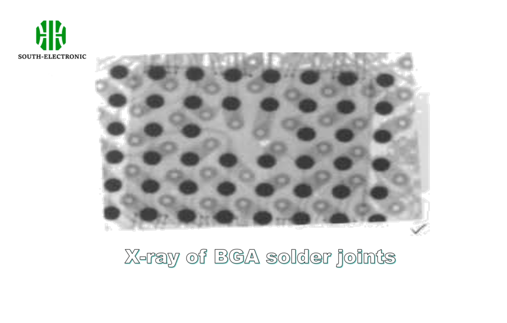
PCB X-ray inspection finds hidden flaws like solder voids, bridges, cracks, and component misalignments inside layers. This non-destructive test sees what eyes and AOI miss. It prevents field failures by checking internal connections.
Transition paragraph:
Knowing what flaws X-rays detect is step one. Next, I’ll explain how to pick the right inspection method for YOUR factory’s budget and needs.
2D vs. 3D vs. CT: Which PCB X-Ray Technology is Right for MY Needs?
Choosing the wrong X-ray tech wastes money. Pick poorly, and you’ll miss critical flaws or overpay. Match your choice to actual needs.
2D suits basic double-layer boards. 3D scans tilted samples for complex BGAs. CT slices through multi-layer boards. Assess your board complexity and acceptable inspection speed first.
Picking Your Power: Depth Matters
Different electronics demand different inspection depth. Simple through-hole components? 2D X-ray gets fine details quick and cheap. Multi-layered boards with hidden vias? You can’t trust it.
I run CT scans on dense server boards. Why? Tiny cracked joints hide between twelve copper layers. But don’t pay for CT if you build power adapters.
| Tech | Best For | Speed | Component Examples | Cost Range |
|---|---|---|---|---|
| 2D | Double-layer boards, SMT parts | Fastest | Resistors, QFPs | $-$$ |
| 3D | Medium complexity, BGA checks | Moderate | BGAs, QFNs | $$-$$$ |
| CT | High-layer PCBs, buried defects | Slow | Stacked ICs, Microvias | $$$-$$$$ |
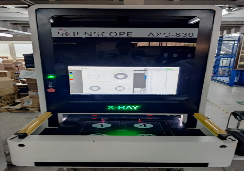
Never skip automated X-ray inspection PCB machines for high volume lines. Manual review is painful.
What key technical parameters matter for PCB x-ray equipment?
Drowning in tech specs? Many focus on resolution, but neglect automation. Ignore key parameters, and you’ll regret reliability.
Resolution (below 1µm for microBGAs), magnification (10,000X+), source voltage, and automation level define performance. Optimize these based on component sizes and output goals.
Beyond Resolution: Hidden Killers
Resolution isn’t just pixel size. Tiny defects in 0201 resistors or 0.3mm pitch BGAs demand below 800nm systems. But resolution alone fails without brightness. Low-powered tubes leave noisy images. Ever tried inspecting dense boards with weak sources? Shadow effects hide voids completely.
Always check:
- Source Voltage: Under 130kV struggles with thick assemblies
- Detector Type: CMOS sensors outperform older CCDs
- Software: Must flag voids automatically, not just show pictures
- Load Capacity: For large panels or heavy fixtures
A high pcb x ray inspection machine price usually reflects stronger sources and better automation ROI. Pair it with flexible magnification.
Why is PCB X-ray inspection costly? How to optimize costs?
Heard the six-figure quotes? X-ray feels expensive. But recall costs cripple factories. Balance upfront investment with reliability returns.
Equipment costs (machines), operation (training/power), and throughput affect price. Optimized layouts and preventive maintenance lower lifetime cost 30-50%.
Cutting Costs Without Cutting Corners
Yes, a new smt x ray machine costs $80,000 to $300,000. Why? Precision tubes. Lead shielding. High-res detectors. But running costs bite harder: idle operators, calibration services, electricity. I cut costs three ways:
| Cost Factor | Why It Matters | Optimization Tactics |
|---|---|---|
| Machine Price | Upfront capital expense | Buy refurbished; lease options |
| Throughput | Idle time = wasted investment | Optimize board staging flow |
| Maintenance | Tube replacements ($10k+) | Preventive cleaning programs |
| Training | Operators misuse settings | Standardized recipes per board |
Always prioritize X-ray inspection for electronic components on critical joints first. Use sampling—not 100% coverage—unless making satellites. Track ROI via reduced recalls.
Conclusion
PCB X-rays spot deadly hidden faults others miss. Match tech to your board needs, prioritize key specs, and optimize operational costs for maximum reliability paybacks.

