
My laptop suddenly shut down while gaming last week. Overheating ruined my gaming session. That experience taught me why specialized PCBs matter. Power-hungry devices need robust circuit boards.
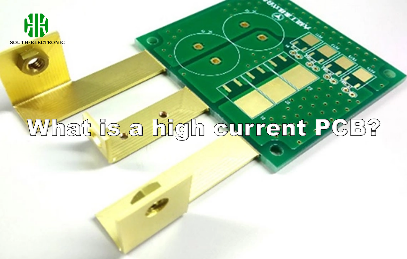
High current PCBs handle over 10 amps electricity using thicker copper traces, multi-layer designs, and thermal vias. They efficiently manage heat in demanding applications like electric cars, industrial machines, and power supplies – unlike basic circuit boards. These specialized boards prevent meltdowns when electricity flows intensely.
Understanding these boards requires digging deeper. Let’s explore three critical aspects every engineer should know.
What materials are suitable for high current PCBs?
My first high current PCB design failed spectacularly. Standard FR-4 material warped under load. Material choice makes or breaks your design.
Copper-clad laminates[^1] with thermal conductivity ratings[^2] above 2.0 W/mK work best, like metal-core (IMS) or ceramic substrates. Polyimide and high-Tg FR-4 handle temperatures above 150°C while thick 4-20oz copper layers reduce resistance. Proper material selection prevents catastrophic thermal breakdown during high-power operations.
Critical Material Properties Comparison
| Property | Standard FR-4 | Metal Core (IMS) | Ceramic Substrate | Why It Matters |
|---|---|---|---|---|
| Thermal Conductivity | 0.3 W/mK | 1-5 W/mK | 20-200 W/mK | Heat dissipation speed |
| Max Temp Rating | 130°C | >200°C | >300°C | Prevents material failure |
| Copper Thickness | 1-2oz | 3-20oz | 3-10oz | Reduces trace resistance |
| Dimensional Stability | Medium | High | Very High | Prevents warping under heat |
| Cost Factor | Low | Medium | High | Budget constraints |
Fifteen years of building power supplies taught me that thermal failures often trace back to improper material choices. When designing high current PCB traces, remember that copper thickness directly impacts current capacity. Doubling copper weight quadruples ampacity. I’ve seen many engineers overlook dielectric thermal resistance – the layer between copper and substrate acts as insulation. For extreme applications, aluminum nitride ceramics outperform popular options despite higher costs. Their astonishing 150-180 W/mK conductivity prevents hotspots around high current pcb terminals.
What manufacturing difficulties exist for high current PCBs?
After ordering my first production batch, the fabricator called: "Your vias are melting!" Manufacturing challenges separate theory from reality.
Thick copper etching requires specialized processes as standard methods undercut traces. Plated holes demand extra copper thickness for high current PCB connectors, while thermal management features[^3] like heatsinks add complexity. Tight impedance control[^4] during lamination becomes critical for multi-layer boards. These steps significantly increase both cost and failure risks compared to regular PCBs.
Production Challenges Breakdown
| Challenge | Standard PCB | High Current PCB | Solution Approach |
|---|---|---|---|
| Copper etching | Easy | Challenging | Differential etching |
| Drill hole wall quality | Tolerant | Critical | Adaptive drilling cycles |
| Layer registration | ±3 mil | ±1 mil | Advanced alignment |
| Thermal warping | Minor issue | Severe risk | Controlled cooling |
| Via reliability | Standard | High maintenance | Filled/vetical vias |
During fabrication, thick copper requires step etching – attacking layers at different rates. I recall one prototype where 10oz copper tore traces due to uneven etching. Another pain point: thermal management compromises during assembly. Z-axis expansion mismatches crack solder joints. Mounting high current pcb terminals needs reinforced anchors – standard pads lift off under stress. The dense copper also presents drilling issues; bit breakage increases 300% with copper layers above 6oz. For high current pcb design, always request impedance coupons and cross-sections before full production. The extra $200 test could save $20k in redesigns.
How to test the reliability of high current PCBs?
My electric skateboard failed mid-hill last summer. No testing equals danger with power systems. Certified test protocols save lives.
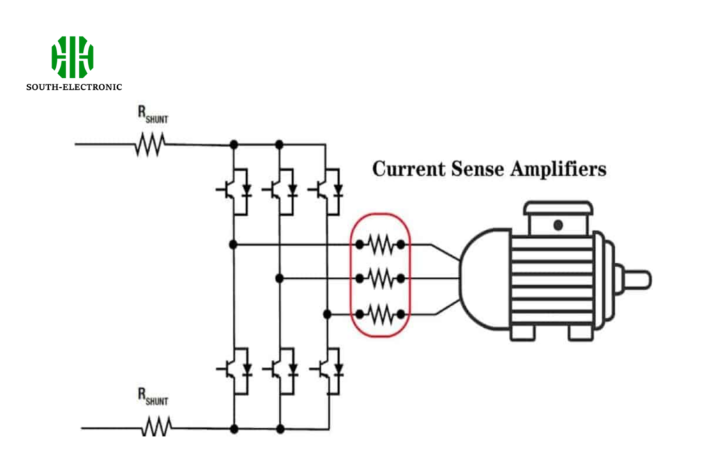
Perform thermal cycle testing from -40°C to +125°C with continuous current loading. Measure resistance instability current terminals, perform IST to check interconnections, and use thermal imaging to find hotspots on traces. These methods validate designs before deployment.
Essential Validation Tests
| Test | Equipment Needed | Pass Criteria | Industry Standard |
|---|---|---|---|
| Thermal Cycling | Environmental chamber | <5% resistance change | IPC-9701A |
| HALT (Highly Accelerated) | Vibration plus temp chamber | No material degradation | MIL-STD-202 |
| Current Burst Test | Programmable power supply | No arcing/discoloration | IPC-2221B |
| Microsection Analysis | Microscopes | Plating voids <10% | IPC-TM-650 |
Validating high current pcb connectors requires specialized environmental chambers during continuous operation. Always test beyond maximum rated capacity – I typically stress equipment at 130% of specification. For high current pcb traces, infrared cameras reveal invisible hotspots in seconds. In one medical device, this caught a 0.3mm trace thinning that traditional methods missed. Finally, perform destructive physical analysis on sacrificial boards[^5]. Cross-sections exposed insufficient plating in my early prototypes, causing catastrophic field failures. Safety margins aren't luxuries – they're necessities in high current pcb design guidelines.
Conclusion
High current PCBs demand specialized materials, precision manufacturing, and thorough testing. Mastering these techniques powers safer electric vehicles and robust industrial systems.
[^1]: Discover how Copper-clad laminates enhance PCB performance and reliability in high-power applications.
[^2]: Learn about the importance of thermal conductivity ratings in PCB materials for effective heat management.
[^3]: Find out how effective thermal management features can prevent failures in high current PCB designs.
[^4]: Understand the importance of impedance control in ensuring signal integrity in high current PCBs.
[^5]: Explore the use of sacrificial boards in testing to prevent costly failures in final products.

