
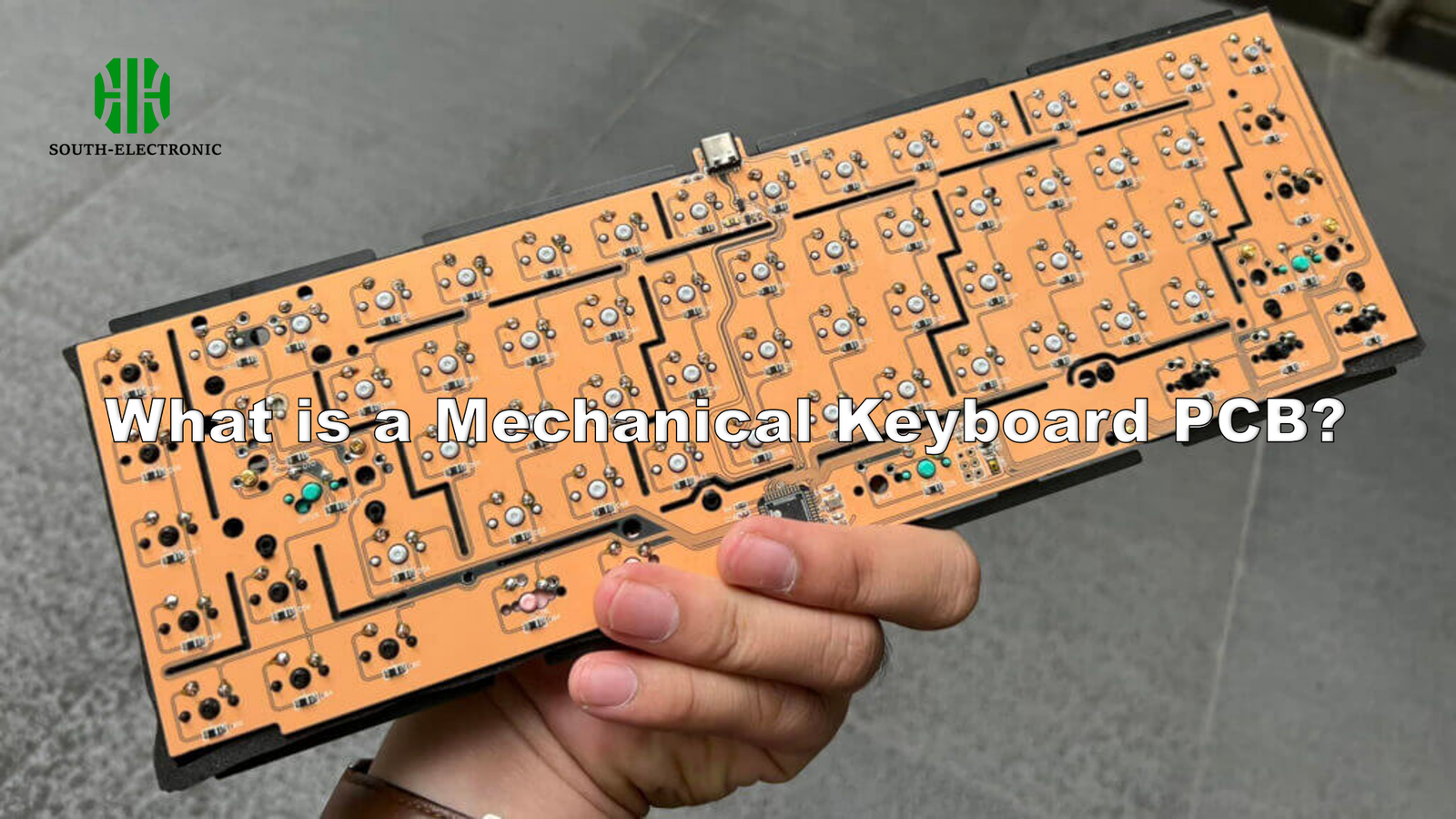
Ever heard your keyboard make noise when you press keys? That clack is more than plastic – beneath your fingers lies a hidden circuit orchestra called the PCB. This unsung hero transforms button mashing into digital magic.
A mechanical keyboard PCB[^1] (Printed Circuit Board) is the brain connecting your switches through copper pathways. It enables customizable layouts[^2], programmable macros[^3], and lightning-fast signal transmission using multi-layer circuit architecture.
)
Before we dive into the copper forests and soldering jungles, let’s unpack why this flat green board defines your typing experience more than any keycap ever could.
The Anatomy of a Keyboard PCB: More Than Just Green Plastic?
Your grandma’s TV remote has circuit boards too – but keyboard PCBs are Formula 1 racing versions. Three components make mechanical boards special:
Mechanical keyboard PCBs consist of switch sockets, diodes for ghosting prevention, and layered signal pathways. Unlike membrane boards, they use through-hole soldering points and customizable matrix layouts to handle complex input combinations.
)
The PCB Trio: Unpacking Core Components
| Component | Function | Why It Matters |
|---|---|---|
| FR4 Substrate | Fiberglass foundation | Handles heat from soldering |
| Copper Traces | Electrical highways | Determines signal speed |
| Solder Mask | Protective coating | Prevents accidental shorts |
The FR4 fiberglass base withstands 350°C soldering temperatures – crucial when attaching switches. Copper traces form customized paths I designed for 60% vs full-size layouts. Excessive trace bending causes latency spikes, which I learned when prototyping my first split keyboard. Solder mask isn’t just green paint – quality coatings prevent crossed signals even when coffee splashes strike.
How Many Layers Do Mechanical Keyboard PCBs Really Need?
Single-layer PCBs work for garage door openers, but keyboards need road networks. My first 40% build failed with 1-layer – inputs randomly triggered neighbors.
Most mechanical keyboards use 2-8 layer PCBs[^4]. Budget boards use 2 layers for basic functions, while enthusiast-grade designs need 4-6 layers for anti-ghosting matrices and RGB lighting circuits.
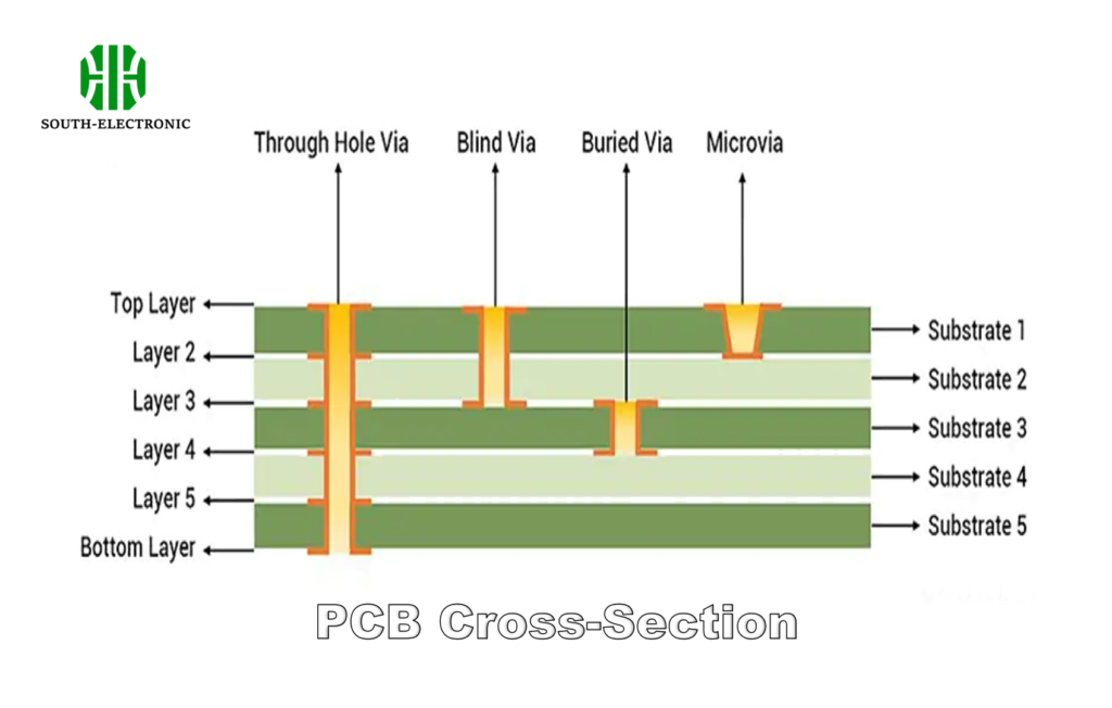)
Layer Warfare: Cost vs Performance
| Layers | Cost | Best For | Limitations |
|---|---|---|---|
| 2 | $ | Basic builds | Ghosting issues |
| 4 | $$ | Gaming boards | Limited RGB zones |
| 6 | $$$ | Enthusiast builds | Complex assembly |
| 8+ | $$$$ | Industrial use | Overkill for typing |
My daily driver uses 6 layers – separate signal and ground planes eliminate interference between keys and RGB LEDs. But when I built my niece’s first keyboard, 2 layers sufficed. The sweet spot? 4-layer PCBs offer 0.5ms faster response than 2-layer in Cherry MX tests.
Which PCB Surface Finish Lasts Longer: HASL vs ENIG vs Gold Plating?
Keyboard spills happen. My coffee disaster killed a HASL PCB but spared the ENIG one – surface finish directly impacts longevity.
ENIG (Electroless Nickel Immersion Gold)[^5] provides the most durable finish, lasting 5-7 years vs HASL’s 2-3 years. Gold plating offers best conductivity but wears faster than ENIG under heavy use.
)
Finish Face-Off: Scratch Test Results
| Finish | Thickness | Oxidation Resistance | Cost Per Board |
|---|---|---|---|
| HASL[^6] | 1-25μm | Poor | $1.20 |
| ENIG | 3-6μm | Excellent | $5.80 |
| Gold | 0.05-0.1μm | Good | $12.00 |
HASL’s uneven surface caused switch alignment issues in my ergonomic build. ENIG’s flat gold layer enabled perfect hot-swap socket placement. For prototypes, I still use HASL – but shipping boards get ENIG. Beware fake ENIG coatings that fail within months. Real ENIG passes 48-hour salt spray tests.
Conclusion
Keyboard PCBs blend engineering and art – layered circuits under polished keycaps determine whether your typing feels like tank battles or ballet.
[^1]: Explore this link to understand the intricate workings of mechanical keyboard PCBs and their impact on performance.
[^2]: Discover how customizable layouts can transform your typing experience and improve efficiency.
[^3]: Learn about programmable macros and how they can streamline your workflow and gaming experience.
[^4]: Understanding the layer requirements for PCBs can help you choose the right design for performance and functionality in keyboards.
[^5]: Explore the advantages of ENIG surface finish, known for its durability and longevity, crucial for reliable keyboard performance.
[^6]: Discover the pros and cons of HASL finish to make informed decisions for your PCB projects, especially for prototypes.

