
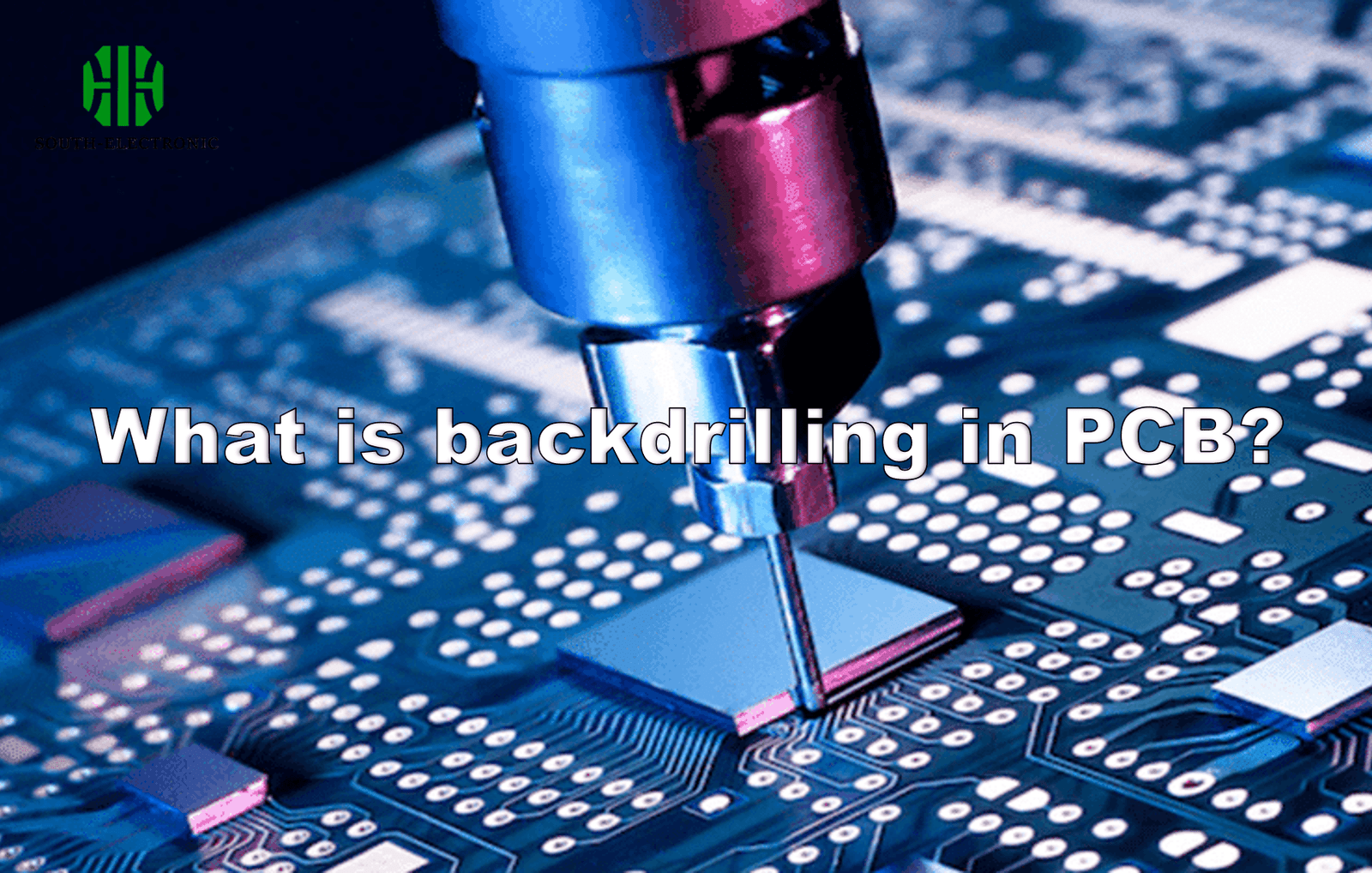
Signal reflections ruining your high-speed PCB performance? Stuck with integrity issues? Discover how backdrilling solves stub problems to rescue your designs.
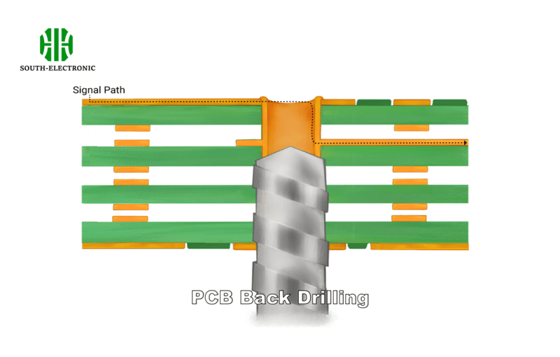
Backdrilling removes unused copper "via stubs[^1]" in multilayer PCBs using controlled-depth drilling from the opposite side. This eliminates signal reflections[^2] at high frequencies, ensuring cleaner transmissions in applications like 5G and server motherboards.
But how exactly does this process work? And does it impact your board’s durability? Let’s break down the critical steps and reliability factors every engineer should evaluate.
How is PCB Backdrilling Performed?
Frustrated by signal distortion from via stubs? Precision back drilling pcb holes requires exact methods to solve impedance mismatches without damaging functional layers.
Manufacturers use a larger drill bit than the original hole, drilling from the backside to a pre-calculated depth. This removes the non-functional copper barrel segment while preserving connections to active layers through meticulous depth control[^3].
Achieving Precision in Back Drilling Process
Three factors determine success:
- Depth Calculation – Based on signal layer requirements
- Registration Accuracy – ±25μm tolerance alignment
- Drill Stability – Vibration control during operation
| Parameter | Impact | Control Method |
|---|---|---|
| Drill Diameter | Must clear copper residue | 0.15mm > original hole |
| Drill Speed | Prevents material tearing | 150-300krpm with peck cycles |
| Depth Tolerance | Prevents layer damage | ±50μm via step-depth control |
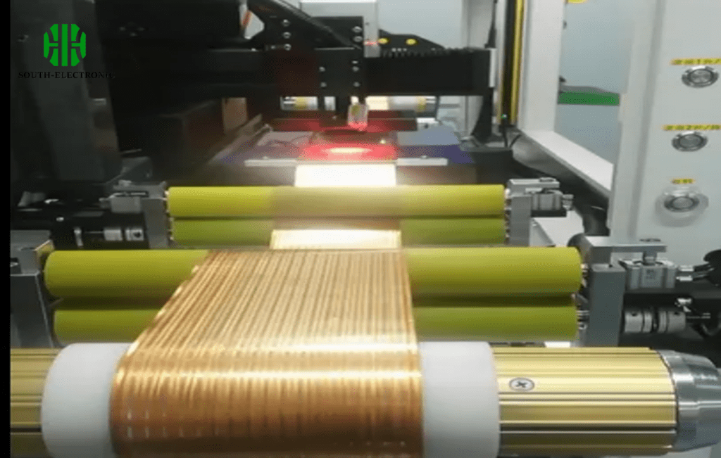
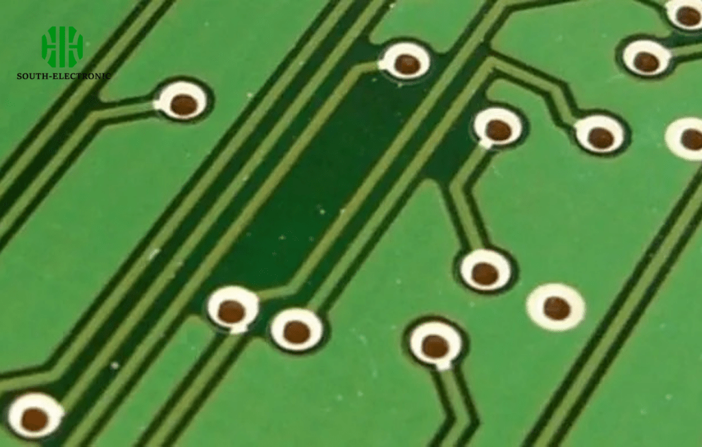
The back drilling process starts with signal analysis identifying problematic stubs. X-ray registration aligns drill targets before CNC machines execute depth-controlled drilling. Post-process microsectioning validates stub removal – we inspect every 10 boards to verify no copper debris remains in critical RF paths.
Does Backdrilling Affect PCB Reliability?
Worried drilling pcb holes weakens your boards? Let’s expose real failure risks versus performance myths.
Properly executed backdrilling maintains PCB integrity. Potential issues like reduced mechanical strength[^4] only occur with incorrect depth control or excessive rework, not standard back drilling sheet metal processes.
Reliability Verifications We Perform
Rigorous tests disprove durability concerns:
- Thermal Stress – 3x solder reflow simulations
- Vibration Testing – 15G resonance scans
- Pull Tests – Compare via strength pre/post-drill
| Failure Mode | Risk Level | Mitigation |
|---|---|---|
| Delamination | Low (±75μm depth variation | |
| Debris Management | Precedes shorts | Manual cleaning processes |
We require suppliers to demonstrate automated depth calibration systems. The best run impedance scans on test coupons from every panel. Avoid shops using universal drilling parameters – each design needs custom calculations. Always request microsections using sequential numbering matching your work order.
Conclusion
Backdrilling eliminates signal-distorting stubs without compromising reliability when performed correctly. Choose suppliers validating every step with quantifiable data.
[^1]: Learn about via stubs and their role in signal integrity to enhance your PCB designs.
[^2]: Explore how signal reflections can impact your designs and learn strategies to mitigate them.
[^3]: Discover the significance of depth control in ensuring successful backdrilling processes.
[^4]: Find out how backdrilling impacts mechanical strength and what to watch for during the process.
[^5]: Understanding thermal cycles is key to ensuring PCB reliability in various environments.
[^6]: TDR testing is essential for verifying stub removal; learn how it ensures quality in PCB production.


