

Ever wonder how your smartphone’s circuits stay protected from dust and moisture? Behind every reliable electronic device lies an unsung hero – PCB ink. This specialized material silently shapes modern electronics manufacturing.
PCB ink[^1] is a customized printing material that forms conductive pathways[^2], insulating layers, and component markings on circuit boards. Its heat-resistant formulations (like solder mask inks[^3]) prevent electrical shorts while enabling precise circuit patterns for devices we use daily.
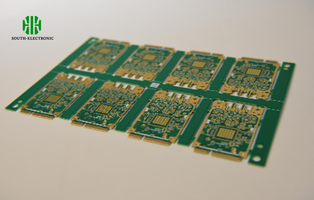
From smartwatches to medical devices, PCB ink determines product reliability. Let’s dissect its critical roles, chemical makeup, and selection strategies through five key questions every engineer should master.
What Is the Purpose of PCB Ink in Circuit Board Manufacturing?
Imagine assembling a circuit board only to discover dust particles causing random shorts. PCB ink eliminates this nightmare through three core functions:
PCB ink creates permanent conductive traces (electrical pathways), protective solder masks (insulation layers), and component identification marks. These functions prevent corrosion, resist soldering errors, and ensure assembly accuracy in devices from 5G routers to EV chargers.
)
From Etching to Precision Printing
- Conductive Inks[^4]
- Replace traditional copper etching: 90% less material waste
- Enable 0.1mm line width vs. 0.3mm with etching
- Table: Traditional vs. Ink-Based Circuit Formation
| Method | Line Resolution | Material Waste | Production Speed |
|---|---|---|---|
| Copper Etching | 0.3mm | 45% | 2 panels/hour |
| Conductive Ink | 0.1mm | 8% | 8 panels/hour |
- Solder Mask Inks[^5]
Block accidental solder bridges on dense IC pads (critical for BGA components) - Legend Inks
White or yellow markings withstand 288°C solder reflow temperatures
What Are the Main Components of PCB Ink?
A smartphone’s solder mask ink blistered after reflow soldering – root cause? Incorrect resin-to-hardener ratio in the ink formula.
PCB ink consists of resin base[^6] (30-50%), hardening agents (15-25%), color pigments (8-12%), and additives (5-10%). These components determine adhesion strength, thermal resistance, and chemical stability – like epoxy resins for automotive boards surviving -40°C to 150°C cycles.
)
Chemistry Behind Performance
Three material science factors govern ink behavior:
-
Resin Matrix
- Epoxy: High temperature resistance (180°C+)
- Acrylic: Fast UV curing (3-8 seconds)
- Polyimide: Flexible circuits (bend radius <2mm)
-
Pigment System
- Titanium dioxide: UV reflectance in white solder masks
- Carbon black: Anti-static properties in conductive inks
-
Critical Ratios
- Resin:Pigment = 3:1 for optimal opacity vs. flexibility
- Solvent content 6H (pencil test)
- Adhesion score 5B (ASTM D3359)
What Factors Should I Consider When Choosing PCB Ink for a Project?
A aerospace contractor chose UL94 V-0 ink but overlooked outgassing[^7] – satellites failed in vacuum.
Select PCB ink based on:
- Operating temperature range
- Adhesion substrate (FR4, ceramic, flex)
- Compliance (UL, IPC-SM-840D, RoHS)
- Processing method (screen vs inkjet)
)
Decision-Making Framework
| Parameter | Consumer Electronics | Automotive | Medical |
|---|---|---|---|
| Temp Resistance | 130°C | 150°C (1000h) | 121°C autoclave |
| Certifications | RoHS | AEC-Q100 | ISO 13485 |
| Cure Speed | 3 min thermal | 2 min UV | 45 min thermal |
| Cost Sensitivity | High | Medium | Low |
Always validate with:
- IPC-4552A[^8] for ENIG compatibility
- 24h humidity testing (85°C/85%RH)
Conclusion
PCB ink selection directly impacts product reliability – match ink properties to operational demands and validate through rigorous preconditioning tests.
[^1]: Explore this link to understand the essential role of PCB ink in ensuring the reliability and functionality of electronic devices.
[^2]: Learn about conductive pathways to grasp their significance in circuit board design and performance, crucial for modern electronics.
[^3]: Discover the importance of solder mask inks in protecting circuits from shorts and enhancing device reliability.
[^4]: Explore how conductive inks can revolutionize PCB manufacturing with less waste and higher precision.
[^5]: Learn about the critical role of solder mask inks in preventing defects in dense IC pads, essential for reliable electronics.
[^6]: Discover the essential components of PCB ink and how they affect performance and durability in electronic applications.
[^7]: Understanding outgassing is crucial for ensuring the reliability of PCBs in vacuum environments, especially for aerospace applications.
[^8]: IPC-4552A provides essential guidelines for ENIG compatibility, ensuring your PCB inks meet industry standards for reliability.

