

For DIY electronics projects, costly PCB fabrication services feel like hitting a brick wall. Prototyping becomes painfully slow. What if you could make circuit boards instantly? This struggle led me to discover PCB milling.
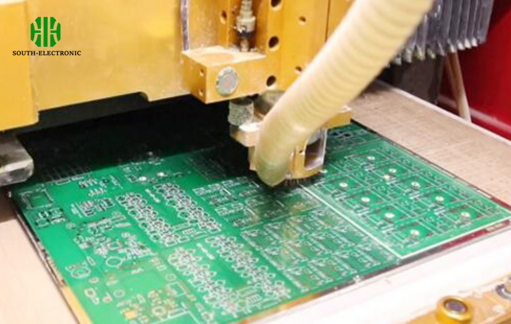
PCB milling is a subtractive process using CNC machines to carve copper-clad boards into custom circuits. It physically removes unwanted copper to create precise traces and isolation paths, perfect for quick prototypes without chemical etching.
Now you know the basics. But uncovering PCB milling’s full potential requires answering deeper questions. Let’s explore critical oversights and practical strategies I’ve learned from years of hands-on work.
Hidden Costs of PCB Milling: Material Waste or Time Investment?
Failed boards pile up quickly during milling attempts. That wasted copper material hurts your budget. Why is waste accumulation unavoidable? Let me share my trial-and-error costs.
Material waste drives hidden expenses, but inefficient milling workflows waste more time. Calculating cost-per-board must include botched attempts and tool replacements.
Cost Comparison: Material vs. Labor Impact
Balancing waste and time requires understanding these key factors:
| Cost Factor | Waste Dominates When | Time Dominates When |
|---|---|---|
| Material Usage | High scrap rates from design errors | Efficient nesting reduces waste |
| Setup Time | Quick material swap | Complex board alignment needed |
| Tool Wear | Dull bits ruin boards (material loss) | Frequent bit changes (time loss) |
| Operator Skill | Novices waste material | Experts minimize adjustments |
Material expenses spike with wrong bit choices. Thin boards break easily. Thick copper requires slow passes. I once wasted 4 boards dialing in depth settings. Time costs grow during intricate designs. Double-sided boards need manual flipping. That alignment added 20 minutes per job. Your shop setup matters too. Bench-top mills handle small boards cheaply. Industrial machines cut larger panels faster but demand pricier bits. Vacuum bed waste reduction helps. Still, tool preservation tops my priority list. Replacing broken $12 bits weekly costs more than monthly copper. Optimize feeds first before purchasing "waste-reducing" gear.
7 Critical Mistakes That Ruin Your Milled PCB
That frustrating moment – your freshly milled board shorts out. Why? Traces rip up or isolation gaps vanish. After debugging 50+ failures, I found consistent culprits.
Incorrect depth settings and dull bits cause most milling disasters. Avoid these 7 errors to achieve reliable boards every time.

Troubleshooting Common Failure Points
Precision avoids tear-outs while balancing speed and quality:
Mistake 1: Poor Copper Clad Preparation
Unclean boards cause slipping. Scrub copper surfaces with steel wool before mounting. Finger oils create adhesion nightmares. I ruined three boards skipping this.
Mistake 2: Wrong Bit Selection
- V-bits (30°-60°): Best for detailed traces under 0.2mm
- Flat end mills: Ideal for outline cuts and large areas
- Down-cut bits: Prevent top-layer chipping
Mistake 3: Ignoring Feeds/Speeds Ratios
My feed/speed chart:
| Material Thickness | Bit Type | RPM | Feed Rate |
|---|---|---|---|
| 0.8mm PCB | 0.3mm V-bit | 24,000 | 150 mm/min |
| 1.6mm PCB | 1mm endmill | 18,000 | 220 mm/min |
Moving too fast shreds traces. Too slow melts laminate. Test settings on scrap pieces. Humidity impacts performance – dry materials behave better.
When Should You Choose PCB Milling Over Manufacturing Services?
Waiting two weeks for shipped PCBs kills project momentum. But milling isn’t always better. From personal projects to client work, timing dictates the winner.
Choose milling for prototypes needing same-day iterations. Use fabrication services for final designs requiring microscopic precision or multi-layer boards.
Decision Guide: Milling vs Outsourcing
Consider these scenarios:
When milling wins:
- 24-Hour Prototyping: Design-test-modify loops within one workday
- Confidential Designs: Sensitive IP never leaves your workshop
- Single/Double Layers: Simple boards under 8 sq. inches
When manufacturers win:
- High Volume: Ordering 50+ boards slashes per-unit costs
- Advanced Features: Requires 4+ layers or impedance control
- Tiny Components: Soldermask/legend under 0.15mm spacing
Milling shines during early development. I fixed five trace routing errors across one afternoon. Manufacturing suits finalized designs. Their silkscreen markings prevent assembly errors. Hybrid approaches work best: Mill version 0.1, produce version 1.0.
Conclusion
PCB milling accelerates prototyping but demands material/tradeoff awareness. Master its nuances, and you’ll bypass fabrication delays while controlling sensitive design.

