
Are you frustrated by hidden PCB defects ruining your electronics? Failed devices cost money. Undetected flaws risk lives. X-ray inspection exposes invisible faults reliably and safely.
PCB X-ray inspection uses penetrating radiation to see inside printed circuit boards. It finds hidden defects like solder voids or cracks in BGA joints without damaging components. This non-destructive testing ensures quality for complex electronics, especially in critical fields like medical devices.
X-rays reveal what eyes cannot see – the internal structure of your PCBs after assembly. Understanding this technology prevents catastrophic failures. Keep reading to learn how X-ray inspection protects high-stakes electronics.
How does X-ray solve BGA solder joint failures?
Ever struggled with intermittent device failures? Faulty BGA connections cause mysterious shutdowns. Thermal stress creates micro-cracks manual checks miss.
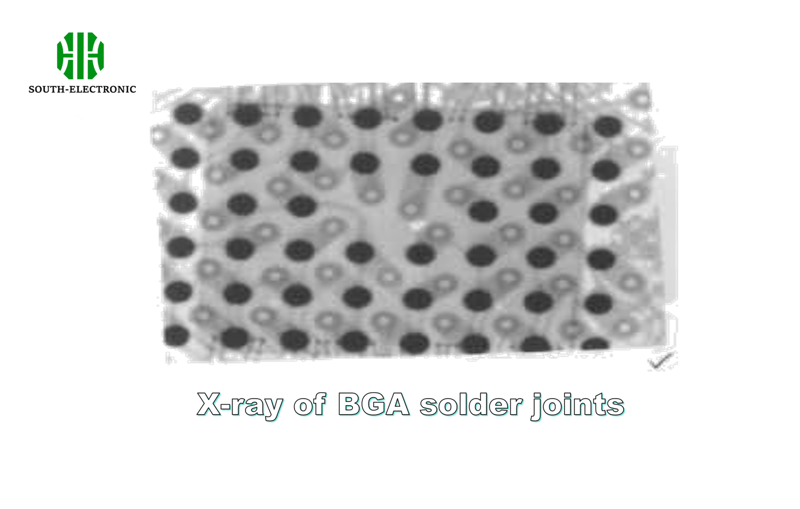
X-ray penetrates packaging to visualize solder joints clearly. It instantly reveals voids, bridging, and ball alignment issues under BGAs, eliminating guesswork.
X-ray imaging captures micron-level details of solder ball connections. It detects hairline cracks, insufficient solder volume, and misalignments invisible externally. This identifies failure risks before devices reach customers.
Pinpointing Hidden BGA Defects
BGA failures cause 37% of electronics returns according to industry studies. Traditional inspection methods often miss:
| Common BGA Failure Modes | Failure Type | Visible? | X-ray Detection | Impact |
|---|---|---|---|---|
| Solder voids | No | Clear voids in ball matrix | Reduced conductivity | |
| Head-in-pillow | Partial | Shows separation | Intermittent disconnects | |
| Cold joints | No | Grainy texture | Early failure | |
| Cracking | Impossible | Fracture lines under balls | Field failures | |
| Bridging | Sometimes | Clear solder merges | Short circuits |
X-ray works because solder absorbs radiation differently than PCB materials. Denser areas like intact solder balls appear dark, while cracks show as bright lines. Modern systems generate 3D layer views, measuring void percentages automatically. This detailed insight helps manufacturers refine soldering profiles and materials for zero-defect production.
Why do medical/aerospace PCBs demand 3D X-ray?
Medical implant failures endanger lives. Rocket circuit errors cause mission disasters. Standard 2D X-ray misses depth-critical flaws.
3D X-ray adds crucial dimension analysis. It maps components layer-by-layer to find microscopic risks conventional methods overlook.
3D X-ray uses computed tomography for depth mapping. It detects internal layer defects, via fills, and lead-free solder voids below 1% tolerance required in aerospace and medical devices.
Why Depth Matters in Critical Systems
Medical/aerospace boards contain stacked components and embedded elements needing volumetric verification:
| Critical 3D Inspection Requirements | Application | 2D Shortfall | 3D Solution | Benefit |
|---|---|---|---|---|
| Cardiac implants | Misses wire depth | Measures coating thickness | Prevents internal corrosion | |
| Satellite boards | Can’t view inner layers | Maps stacked microvias | Ensures signal integrity | |
| Surgical tools | Blurry multi-angle | High-res slices | Verifies conformal coating | |
| Aircraft controls | Blind to voids under shields | Void % calculations | Prevents thermal failure | |
| Deep-space gear | No volumetric data | 3D CAD comparison | Validates hermetic seals |
NASA requires 10μm resolution for Mars rover electronics – impossible with 2D systems. 3D tomography achieves this by rotating boards while capturing hundreds of projections. Specialized software then reconstructs internal geometry. This proves every millimeter of conformal coating coverage or detects thermal expansion voids that might crack during cryogenic space travel.
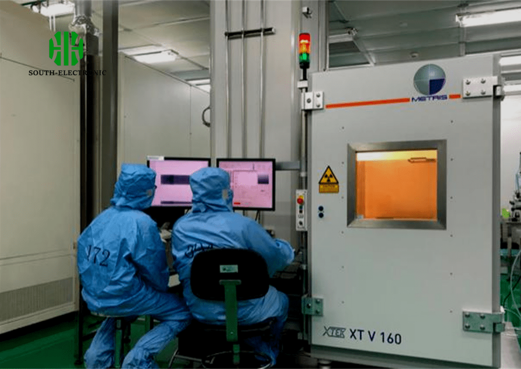
What are the 5 critical specs for choosing a PCB X-ray machine?
Picking wrong X-ray equipment wastes thousands. Overspec models add unnecessary cost while underpowered units miss critical defects. Know exact parameters.
Resolution, voltage, magnification, detector type, and software features determine inspection accuracy. Match specs to board complexity.
Essential specs are resolution below 1μm for BGAs, 130kV tube voltage for dense boards, geometric magnification over 5000×, digital detectors above 10fps frame rate, and automated defect analysis software.
Matching Specs to Inspection Scenarios
Avoid overspending or inadequate detection:
| Specification Optimization Guide | Parameter | Low-End Choice | Ideal Option | Use Case Value |
|---|---|---|---|---|
| Resolution | 5μm | ≤1μm | Micro BGA underfills | |
| Voltage | 90kV | 100-130kV | Multi-layered boards | |
| Geometric Mag | 1000× | ≥5000× | 01005 components | |
| Detector | CMOS/15fps | Digital/30fps | Fast production lines | |
| Software | Basic | AI defect library | Automated pass/fail |
Maximum voltage determines penetration capability. For thick boards containing large capacitors or metal shields, 90kV units fail while 130kV units penetrate. Resolution impacts observable detail – 10μm systems miss microcracks in 0.3mm pitch BGAs that 1μm systems catch. Always verify detector frame rates match production speed demands. Slow detectors create bottlenecks on high-volume lines needing <30-second inspection cycles.
Conclusion
X-ray inspection locates hidden PCB defects effectively. It ensures reliability for vital electronics like medical implants and aerospace controls. Advanced 3D systems provide critical depth analysis.

