

Ever wondered what that colored coating on circuit boards does? Without it, your electronics would quickly fail.
Solder mask is a protective polymer layer on a PCB that prevents short circuits by insulating copper traces and stopping solder bridges. It shields the copper from environmental damage, ensuring the board's reliability and extending its lifespan.
Understanding solder mask is key to appreciating PCB reliability. Let's dig deeper into what this essential layer does and why it matters so much for all our electronic devices.
What Is Dry Film Solder Mask?
Are you curious about different solder mask types? Not all masks are applied the same way.
Dry film solder mask is a photographic film applied to PCBs, cured by UV light, and then developed. It offers high resolution and uniform thickness, making it ideal for fine-pitch components and high-density boards.

Dry film solder mask, or DFSM, is a common method for applying this protective layer. I see it as a specialized sticker for circuit boards. Unlike liquid solder mask which is sprayed or screen-printed, DFSM comes in sheets. The process starts with the film being laminated onto the PCB under heat and pressure. Then, a phototool with the desired pattern is placed over it, and the board is exposed to UV light. This light hardens the exposed areas. The unexposed areas are then washed away in a developer solution, leaving the solder mask only where it's needed—over the traces and pads. This technique allows for very precise patterns, which is critical for modern PCBs with tiny components. I've seen firsthand how this precision impacts the final product, especially with boards that have extremely small features. It’s like using a stencil that guarantees perfect alignment every time. This method significantly reduces the chance of errors that could lead to shorts on densely packed boards. The consistency it provides across the entire surface is also a major advantage, ensuring uniform protection.
| Feature | Description | Benefit |
|---|---|---|
| Application | Laminated as a sheet under heat and pressure | Uniform thickness, fewer air bubbles |
| Curing | UV light exposure followed by developing | High resolution for fine-pitch designs |
| Thickness | Consistent across the board | Reliable insulation even on complex boards |
| Cost | Can be higher for small runs | Justified for demanding applications |
Why Are PCBs Usually Green?
Have you ever wondered why most circuit boards are green? It’s not just a random choice.
PCBs are usually green because green solder mask offers the best contrast for inspection, is cost-effective to produce, and has been the industry standard for decades. This color helps technicians spot defects more easily.

The prevalence of green PCBs isn't just about aesthetics; it's rooted in practical reasons and historical standards. I remember when I first started in electronics, every board I saw was green, and I just accepted it. However, the green pigment in the solder mask provides excellent contrast for visual inspection. This contrast makes it easier for both human eyes and automated optical inspection (AOI) machines to identify issues like solder bridges, missing components, or incorrect polarity. Green also has historical significance; it was one of the first reliable and readily available colors for solder mask chemicals, establishing it as a de facto industry standard. Over time, manufacturing processes became optimized for green, making it the most cost-effective option for many producers. While other colors like blue, red, or even black are available now, green remains the most common choice due to these combined factors. It’s a color that signifies reliability and ease of manufacturing. For me, seeing a green PCB always brings a sense of familiarity and trust, knowing that it’s built on decades of industry practice. The choice of green really boils down to balancing visibility, cost, and historical precedent. It’s a subtle but powerful example of how practical considerations shape the electronics we use every day.
| Aspect | Reason for Green Solder Mask | Impact |
|---|---|---|
| Visibility | Provides strong contrast against copper traces and silkscreen | Easier for manual and automated inspection |
| Cost | Most optimized and cheapest to produce due to historical use | Reduces manufacturing costs |
| Industry | Established as a long-standing industry standard | Familiarity and widespread adoption in production |
| Eye Fatigue | Less strenuous on the eyes during long inspection periods | Improves worker comfort and reduces errors |
How Do I Know If My Solder Mask File Is Correct?
Are you worried your PCB design might have solder mask issues? Getting it right is crucial.
You can check your solder mask file by carefully reviewing the Gerber files, paying attention to clearances, and ensuring all pads and vias have the correct openings. Use a Gerber viewer to overlay the mask layer with the copper layers.
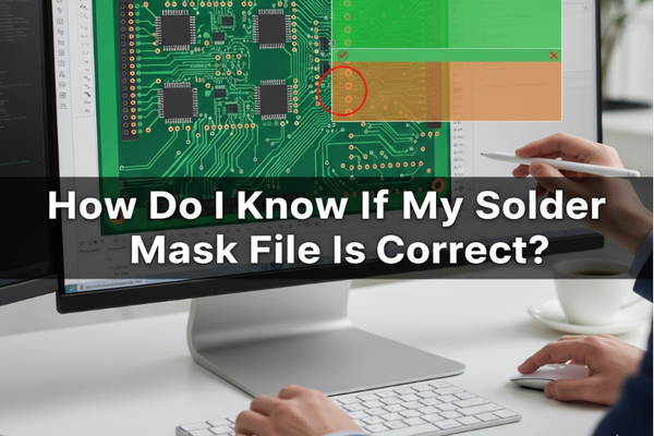
Ensuring your solder mask file is correct is a critical step before sending your PCB design for manufacturing. I've learned that overlooking this can lead to expensive re-spins. The primary way I verify it is by meticulously reviewing the Gerber files. I use a Gerber viewer to load my copper layers and then overlay the solder mask layer. The key things to look for are clearances around pads. The solder mask opening should be slightly larger than the copper pad it exposes. This ensures the mask doesn't encroach on the pad, which could prevent proper soldering. This is often called a "solder mask clearance" or "solder mask expansion." Also, check that non-plated through-holes (NPTH) often have a solder mask opening, while plated through-holes (PTH) that need to be covered by solder mask (e.g., for via-in-pad designs) are properly tented. Pay attention to small features and tight spaces to ensure the mask doesn't create unwanted bridges or completely cover tiny pads. Many EDA tools have design rule checks (DRC) that include solder mask rules, which can catch common errors automatically. I also double-check the board's edge to make sure the solder mask is not too close, which can lead to peeling. This detailed review prevents costly mistakes later in the production process and saves a lot of headaches.
| Check Point | What to Look For | Why it Matters |
|---|---|---|
| Clearance around Pads | Solder mask opening slightly larger than the copper pad | Prevents mask from covering pad, allows good solder joint |
| Via Tenting | Vias intentionally covered by solder mask | Prevents solder wicking, protects vias from corrosion |
| Solder Mask Bridges | Mask material separating adjacent pads or traces | Prevents short circuits from solder bridging |
| Gerber File Overlay | Visual inspection of mask layer over copper in a viewer | Catches discrepancies not caught by DRC |
Conclusion
Solder mask is essential for PCB integrity. It prevents shorts, protects copper, and aids assembly, making electronics reliable and durable.

