
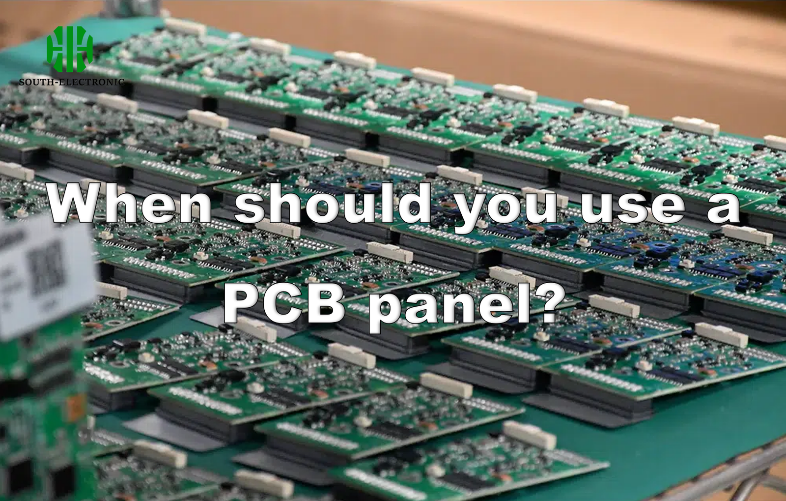
Ever tried fitting tiny PCBs into assembly lines? It’s frustrating, inefficient, and costly when handling small boards individually. Why waste time when there’s a smarter solution?
Use PCB panels when manufacturing large quantities of small or irregularly shaped boards. Panelization boosts efficiency, cuts production costs, simplifies handling during assembly, and protects components near board edges for consistent quality.
Now let me show you exactly how panelization transforms manufacturing – and what pitfalls to avoid during the process. We’ll explore reliability impacts, break down connection methods, and uncover hidden production challenges.
Does panelization affect PCB reliability?
Worrying about panelization weakening your boards? Many believe joining PCBs sacrifices structural strength. I’ve seen engineers hesitate over imaginary break points.
Panelization itself doesn’t harm PCB reliability if properly designed. Strategic routing and clearance rules prevent stress concentration. Correctly applied, it actually protects vulnerable edge components during handling and assembly processes.

Three reliability factors in panel design
| Factor | Risk | Mitigation |
|---|---|---|
| Edge Stress | Fractures near separation points | 5mm clearance zone rules |
| Thermal Distortion | Warping during reflow | Balanced copper distribution |
| Vibration Damage | Component detachment in routing | Mouse bite reinforcements |
Proper PCB panel design guidelines solve all three issues simultaneously. I always consider how depanelization forces spread across the panel array. That means placing no vias or traces within the critical 3-5mm stress buffer zone. We distribute sensitive components toward the panel’s center, creating natural shock absorbers. Reliable panels also require material uniformity – inconsistent copper density causes uneven heating during soldering. By balancing the copper layers, we prevent warping that cracks solder joints. Finally, I implement breakaway tab anchors at high-mass component locations so vibrations during cutting won’t dislodge chips. These techniques transform panels from liability to durability assets.
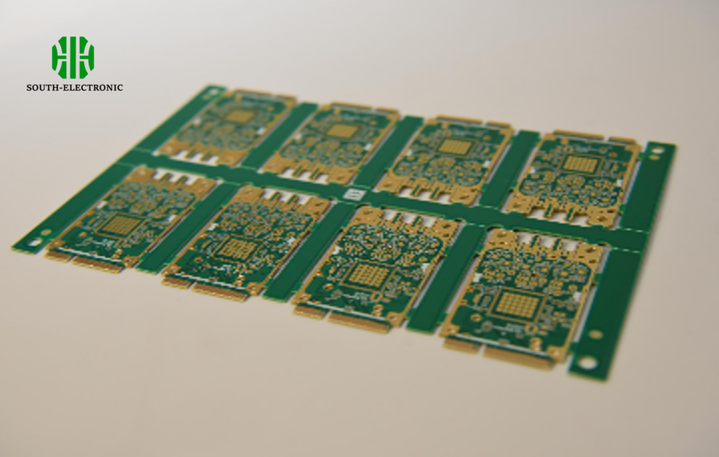
What are the differences between V-cut, mouse bites, and breakaway tabs?
Struggling to choose between connection methods? Each technique suits different board requirements. Wrong choices mean cracked boards during separation.
V-cut creates continuous grooves for straight-line separation. Mouse bites use perforated holes for complex shapes and thin boards. Breakaway tabs connect boards with thinner supporting tabs for stress-controlled manual removal.

Choosing the right connection method
| Method | Best For | Thickness | Separability | Cost |
|---|---|---|---|---|
| V-cut | Rectangular panels | 0.8mm+ | Automated | Lowest |
| Mouse Bites | Irregular shapes | Any | Semi-auto | Medium |
| Breakaway Tabs | Sensitive areas | 1.0mm+ | Manual | Highest |
The PCB panel V cut works through continuous 30-60 degree angled grooves sliced through 1/3 of the board’s thickness. Ideal for standard rectangles – I’ve used them 90% of time for smartphone boards. But be cautious: sharp V-cuts concentrate stress on corners. Mouse bites solve that through perforated micro-holes along separation lines. Though requiring extra drilling costs, their honeycomb pattern lets me create organic pcb panel shapes while preventing tear propagation. Breakaway tabs become essential when boards can’t undergo vibration. Think flight control PCBs with BGAs. The method connects panels through several 1mm-thick bridges that snap cleanly by hand – but require manual labor that scales poorly beyond prototypes. Always match the method to your panel size, geometry and automation level.
What manufacturing challenges exist for PCB panels?
Ever received warped, unusable PCB panels? Common issues derail production when overlooked. 30% of "sudden" defects actually stem from poor panelization planning.
Key challenges include maintaining dimensional stability during routing, preventing tool breakage on dense arrays, minimizing material waste, and ensuring separation consistency with zero board damage across production volumes.
Solving 4 core manufacturing challenges
| Challenge | Problem Source | Solution |
|---|---|---|
| Panel Warping | Uneven copper distribution | Symmetrical layer stackup analysis |
| Router Damage | High-density tool paths | 30% glass-reinforced materials |
| Yield Loss | Bad nesting efficiency | Auto-array optimization software |
| Fractures | Inconsistent separation | Laser-cut calibration standards |
Achieving flawless PCB panelization starts with understanding thermal dynamics. I’ve learned that copper imbalance causes most warping – where one layer expands more than others during soldering. My shop runs DFM checks enforcing <15% copper density variation across layers. Router bit breakage drops dramatically when we increase fiberglass content in substrate materials. High-density pcb panel arrays require particularly precise tool paths. For material efficiency, I never arrange boards intuitively. Nesting software squeezes production costs by optimizing every millimeter – saving 22% material last quarter on wearable PCBs. The final hurdle? Separation consistency. We calibrate V-cut depths weekly using laser micrometers because blades wear faster than operators realize. Temperature-controlled separation rooms prevent resin brittleness too. These measures ensure all de-paneled boards meet IPC-A-610 Class 3 standards.
Conclusion
Use PCB panels when producing compact boards in volume. Proper design enhances reliability and cost efficiency while preventing manufacturing defects. Choose connection methods based on board shape and separation needs.

