
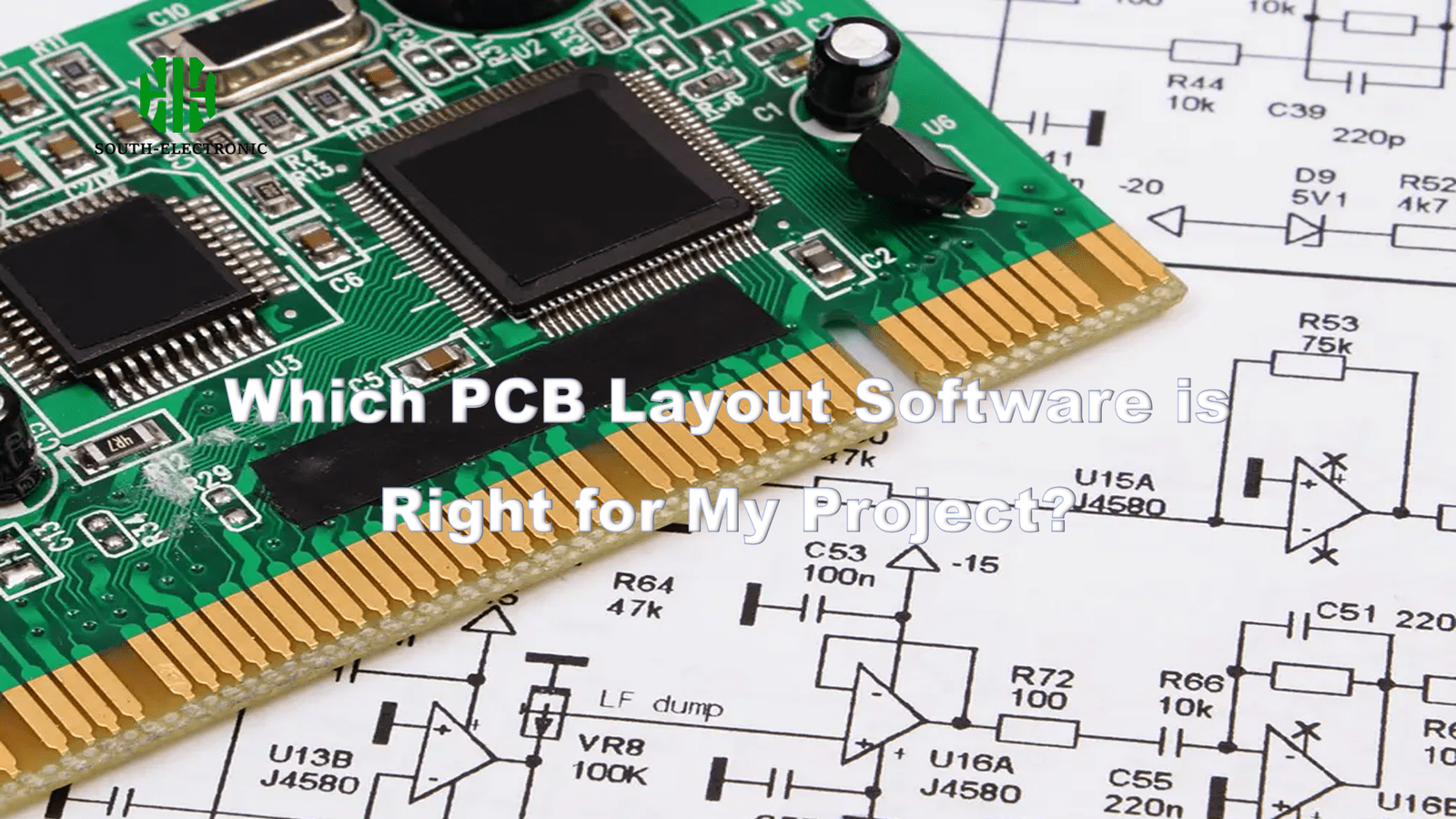
Struggling to pick PCB layout tools? Your deadline looms as options overwhelm. I faced this paralysis with my first circuit board project. The right choice saves time and prevents redesigns.
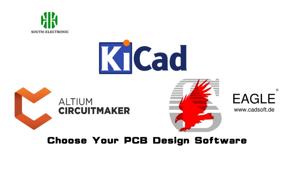
Match software to your project scale. For simple pcb projects, try free pcb design tools[^1] like KiCad or EasyEDA. Complex designs like computer motherboard design need Altium or Allegro. I use budget and complexity as my main filters.
Now explore key considerations before selecting your pcb design online platform. These insights come from burning midnight oil on flawed layouts.
Top 10 PCB Design Rules You Can’t Afford to Ignore?
Ever lost a prototype to avoidable errors? I fried three boards ignoring trace spacing. Basic rules prevent 80% of pcb layout failures.
Follow these non-negotiable standards: maintain clearance between traces, avoid 90° angles, and separate analog/digital grounds. Consistent rule checks in your pcb layout software prevent costly respins.
Core Principles for Reliable Circuit Boards
Stable power delivery keeps circuits humming. I learned this through flickering LEDs in early pcb projects. Three fundamentals matter most:
-
Power Integrity
- Use wider traces for power lines
- Place decoupling capacitors near ICs
- Layer dedication improves stability
-
Signal Quality
Issue Fix Crosstalk Increase trace spacing EMI Add ground planes Impedance mismatch Calculate trace width -
Thermal Management
Copper pours act as heat sinks. For high-power components, I now use thermal vias. Spacing components aids airflow and prevents hotspots during operation. Fusion 360 pcb design shows live thermal simulations.
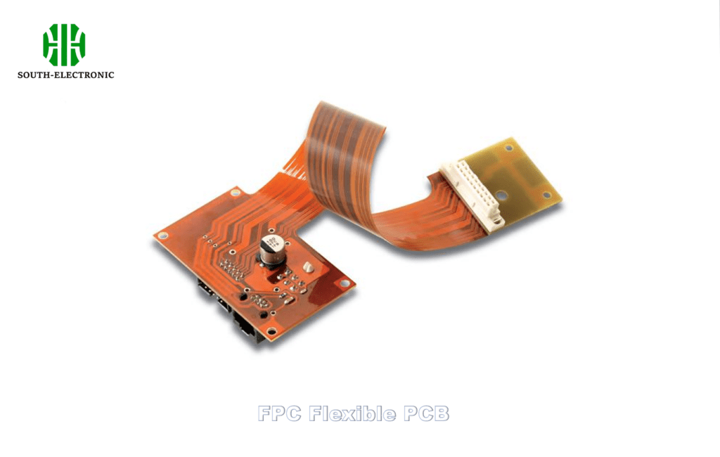
What Makes Flex PCB and Motherboard Layout Design So Challenging?
Why do professionals dread flex pcb design? My first flexible circuit snapped during testing. These boards demand different physics understanding.
Flex circuits tolerate bending but crack if stressed incorrectly. Motherboards pack dense components tightly. Both require specialized layer planning and 3D modeling unavailable in basic free pcb design tools.
Overcoming Flexibility and Density Hurdles
Computer motherboard design feels like micro-surgery. These projects demand advanced approaches:
-
Flex PCB[^2] Survival Tactics
Bend radius calculations prevent fractures. I use sandwich structures for multi-layer flex designs. Stiffeners reinforce connection points. Flexible sections never host critical ICs. -
Challenge Solution Signal integrity Extensive simulation runs Power delivery Multi-phase VRM placement Thermal hotspots Strategic copper balancing -
Tool Limitations
Free pcb layout software often lacks HDI support[^4]. High-density projects require Altium or Cadence. I simulate mechanical stresses in Fusion 360 pcb design before printing.
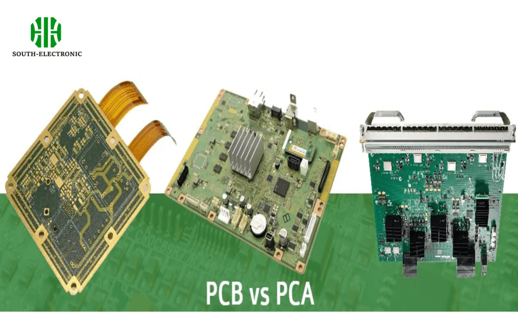
PCA vs PCB: What’s the Difference? And How Are PCB Classes Defined?
Confused when vendors mention "PCA"? I mistakenly ordered bare boards for assembly. Understanding these terms prevents project delays.
PCBs are bare circuit boards without components. PCA[^5]s (Printed Circuit Assemblies) have mounted parts in pcb design. IPC standards[^6] define three pcb class[^7] levels for reliability.
Decoding Manufacturing Terminology
Choosing wrong pcb class killed my drone project. Breaking down specifications clarifies decisions:
-
Functional Differences
- PCB: Unpopulated laminate board
- PCA: Functional electronic unit
Testing occurs at PCA stage always
-
IPC Standard Classes Class Use Case Tolerance 1 Consumer electronics +/- 20% 2 Industrial equipment +/- 10% 3 Aerospace/medical +/- 5% -
Impact on Design Workflow
Higher classes demand stricter pcb layout rules. Class 3 requires cleanroom assembly and automated optical inspection. I always specify class during online pcb design ordering now.
Conclusion
Your project needs dictate the best pcb layout software. Match tool capabilities to complexity and budget for optimal results every time.
[^1]: Explore this link to discover top free PCB design tools like KiCad and EasyEDA that can simplify your projects.
[^2]: Explore this link to understand the unique challenges and solutions in Flex PCB design, enhancing your knowledge in this specialized field.
[^3]: Discover insights into the intricate challenges of motherboard design and how to tackle them effectively.
[^4]: Learn about the significance of HDI support in PCB design and how it impacts high-density projects.
[^5]: Understanding PCA is crucial for ensuring your project has the right components and assembly, preventing costly mistakes.
[^6]: Exploring IPC standards will help you grasp the reliability levels required for your specific project needs.
[^7]: Learning about PCB classes can significantly impact your design decisions and project success, ensuring you choose the right specifications.


