
Choosing PCB software feels overwhelming? Too many options exist. Don’t let poor tools ruin your project. I faced this confusion early in my career. Let me guide you through the maze.
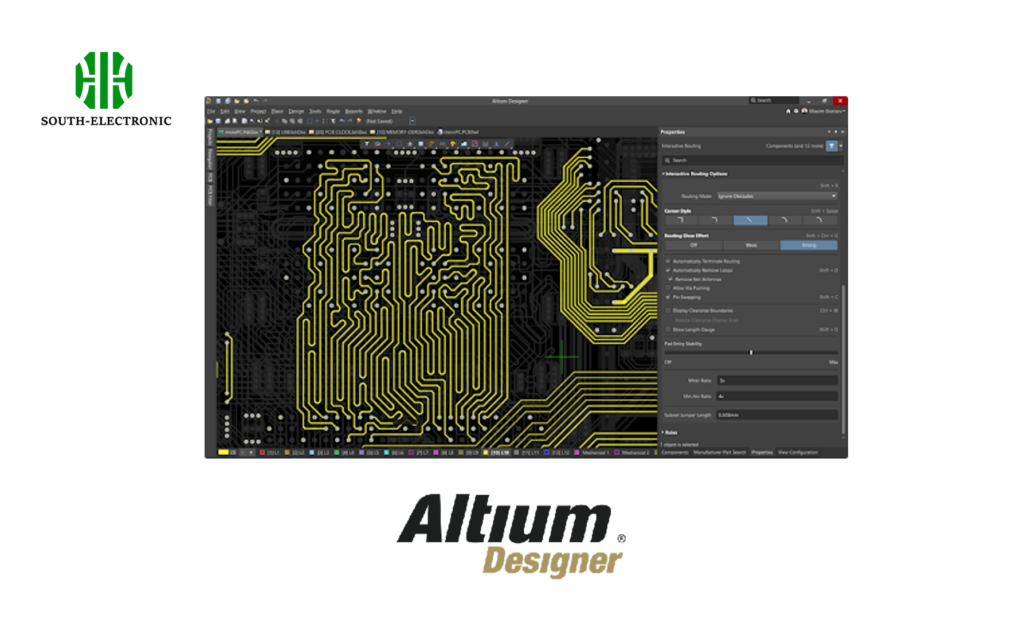
Altium Designer dominates the professional market for complex designs due to its unmatched features, while KiCad and Autodesk EAGLE lead among free and low-cost PCB design softwares. These tools balance power and accessibility for different needs.
Whether you’re a hobbyist or engineer, finding the right software transforms your workflow. Below, I break down costs, free options, Altium accessibility, and production tips to help you succeed.
How much do PCB software cost? What free tools are available?
Stressed about PCB software budgets? Costs shouldn’t block innovation. I’ve tested paid and free solutions side-by-side. Affordable paths exist for every project.
High-end PCB CAD software like Altium costs $7,000+ per license, but free tools like KiCad offer full features at zero cost. EAGLE provides mid-tier subscriptions ~$500/year, striking a balance for small teams and best free pcb design softwares seekers.

Pricing Breakdown and Free Alternatives
PCB design softwares vary wildly in price. Don’t commit without understanding the landscape. Here’s a direct cost comparison:
| Software | Cost Range | Ideal For |
|---|---|---|
| Altium Designer | $7,000 – $10,000 | Complex professional projects |
| Autodesk EAGLE | Free – $510/year | Hobbyists & education |
| KiCad | Free forever | Startups & beginners |
KiCad remains the top free pcb design software, with no hidden fees. It handles multilayer boards and has active open-source updates. EAGLE’s free version supports two-layer designs but limits board size. For small budgets, KiCad delivers shockingly powerful tools comparable to paid options. Always test free softwares para pcb before investing. Remember, student versions from Autodesk or Altium slash costs significantly.
Can I use Altium for free?
Wish you could try Altium without emptying your wallet? Instant access sounds perfect. I once hunted for loopholes myself. Unfortunately, free permanent access doesn’t exist—but alternatives do.
Altium lacks a long-term free version, with trials limited to 15 days. However, its student program grants low-cost access. For permanent $0 solutions, KiCad provides similar core features among best free pcb design softwares.
Trial Limits and Practical Workarounds
Breaking down Altium’s accessibility clarifies real-world options. Consider these three approaches:
- 15-Day Trial: Full feature access—ideal for urgent project testing. Downside? Short deadline pressures you.
- Altium Education: Schools get discounts via academic partnerships. Confirm your institution’s eligibility first.
- Free Alternatives: KiCad mimics 90% of Altium’s functionality without cost. It exports industry-standard Gerber files and supports complex layouts.
For softwares de diseño de pcb, EAGLE’s affordable subscription bridges gaps between free KiCad and premium Altium. If abandoning Altium, replicate its functions through KiCad’s schematic capture and autorouter. Always prototype using available free pcb design softwares before scaling to paid tools.
How to export production files? What DFM rules need attention?
Panic about manufacturing delays? One wrong export kills your prototype. I wasted weeks fixing file formatting. Master these steps to avoid costly mistakes.
Export Gerber, drill files, and assembly drawings using standard formats like RS-274X. Critically follow DFM rules: space clearances (>0.2mm), solder mask openings, and annular ring widths to prevent pcb cad software-related failures.

File Export Essentials and DFM Compliance
Exporting production files requires precision. Softwares used for pcb design generate outputs—but you must configure settings. Break it into two phases:
-
File Export Protocol
- Generate Gerber files for each copper layer
- Include drill files in TXT or EXCELLON formats
- Attach component centroid (XY) files for SMT assembly
-
Key DFM Rules Table Rule Minimum Value Failure Risk Trace Spacing 0.2mm Electrical shorts Hole Pad Ratio 0.3mm annular ring Broken connections Silkscreen Clearance 0.1mm Assembly errors
Use in-pcb CAD software DRC checkers to automate DFM violations. KiCad and Altium flag clearance errors instantly. Avoid tiny text sizes under 0.8mm for readability. Finally, email outputs to your manufacturer early—this validates softwares para pcb compatibility!
Conclusion
Choose PCB software matching your needs: Altium for pros, EAGLE for learners, or KiCad for $0 projects. Prioritize DFM compliance to accelerate production—start simple with free tools today.

