
In electronic products, printed circuit boards (PCBs) are like the nervous system, connecting various electronic components. The surface treatment of PCBs not only affects the performance of the PCB but also the stability and lifespan of the electronic product. Today, we’ll take a deeper look at PCB surface treatment processes.
Why PCB Surface Treatment?
PCBs are primarily made of copper, which easily oxidizes in air, forming copper oxide. Copper oxide not only affects the solderability of the PCB but also reduces its conductivity and reliability. Therefore, to protect the copper layer and improve the performance of the PCB, PCB surface treatment is necessary.
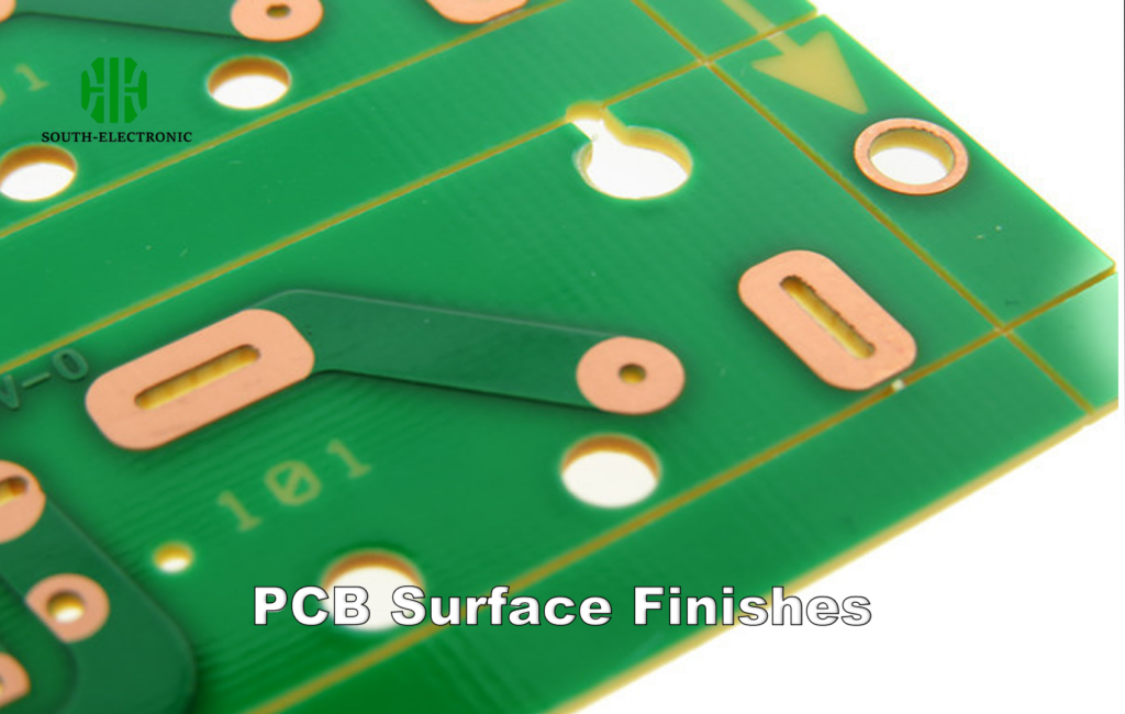
Common PCB Surface Treatment Processes
- Hot Air Leveling (HASL)
Hot air leveling, also known as hot air solder leveling, is a relatively traditional surface treatment process. It involves immersing the PCB in molten tin-lead solder and then using heated compressed air to flatten the solder, forming a uniform solder coating on the PCB surface. This process can be divided into vertical and horizontal methods. The horizontal method is generally considered preferred because it produces a more uniform coating and can be automated.

- Organic Coating (OSP)
The organic coating process chemically grows an organic film on a clean, bare copper surface. This film is resistant to oxidation, thermal shock, and moisture, protecting the copper surface from further rusting in normal environments. It can also be easily removed by flux during the subsequent high soldering temperatures, making soldering easier.
- Electroless Nickel/Immersion Gold (ENIG)
Electroless nickel/immersion gold (ENIG) coats the copper surface with a thick, electrically conductive nickel-gold alloy, providing long-term protection for the PCB. The primary function of the nickel plating is to prevent interdiffusion between gold and copper. Without the nickel barrier, gold would diffuse into the copper within hours. Furthermore, nickel enhances the coating’s strength, controls Z-direction expansion at high temperatures, and prevents copper dissolution, facilitating lead-free soldering.
- Immersion Silver (ENIG)
The ENIG process lies between OSP and electroless nickel/immersion gold. It forms a nearly submicron-thick, pure silver coating on the PCB surface through a replacement reaction. Sometimes, organic matter is included in the immersion silver process, primarily to prevent silver corrosion and mitigate silver migration.
- Immersion Tinning
The immersion tinning process uses a chemical replacement reaction to coat the copper surface of a PCB with a layer of tin. Since all current solders are tin-based, the tin layer is compatible with any type of solder. In the past, tin whiskers were prone to forming on PCBs after immersion tinning. During soldering, these whiskers and tin migration caused reliability issues, limiting the application of immersion tinning. Later, organic additives were added to the immersion tin solution, resulting in a granular tin layer. This overcomes these issues while also providing excellent thermal stability and solderability.
How to Choose a PCB Surface Treatment
Choosing the appropriate PCB surface treatment requires comprehensive consideration of several factors:
- Application Scenario:
Different electronic products have different PCB performance requirements. For example, high-end electronic products such as mobile phones and computers typically require high flatness, solderability, and electrical performance, and may choose electroless nickel plating or immersion gold plating. Consumer electronics, such as small digital devices, are more cost-sensitive and may opt for hot air leveling or immersion tin.
- Cost:
The costs of different surface treatment processes vary significantly. Hot air leveling is relatively low, while processes such as electroless nickel/immersion gold plating and electroless nickel-gold plating are relatively expensive. When choosing a surface treatment, you need to weigh the product’s pricing and market demand.
- Environmental Requirements:
With increasing global environmental awareness, environmental requirements such as lead-free and halogen-free are becoming industry standards. Therefore, when selecting a surface treatment process, it is important to consider whether it complies with relevant environmental regulations and customer requirements. For example, hot air leveling using lead-containing solder will not meet environmental requirements, while processes such as organic coating, immersion silver, and immersion tin are relatively more environmentally friendly.
- Solderability:
If the product requires high-volume soldering, it is important to choose a process with good solderability, such as hot air leveling or immersion tin. Organic coating, on the other hand, requires removal of the coating before soldering and may not be suitable for large-scale soldering.
- Storage Conditions and Duration:
If PCBs need to be stored in harsh environments for extended periods, a process with good corrosion resistance and a long shelf life, such as electroless nickel plating or immersion gold plating, should be selected. OSP, on the other hand, has a shorter shelf life and is not suitable for long-term storage.
There are many different PCB surface treatment processes, each with its own unique advantages and disadvantages and applicable scenarios. In practical applications, it is necessary to consider various factors based on specific needs to select the most appropriate surface treatment process to ensure the performance of the PCB and the quality of the electronic product.

