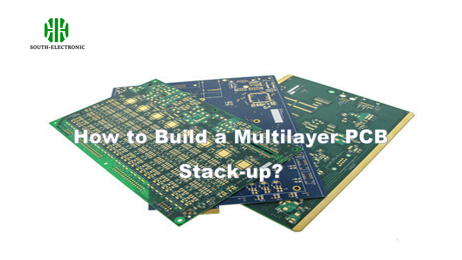
Master multilayer PCB stack-ups with strategic layer sequencing, material selection, and EMI mitigation for optimal signal, thermal, and manufacturing performance.

Master multilayer PCB stack-ups with strategic layer sequencing, material selection, and EMI mitigation for optimal signal, thermal, and manufacturing performance.
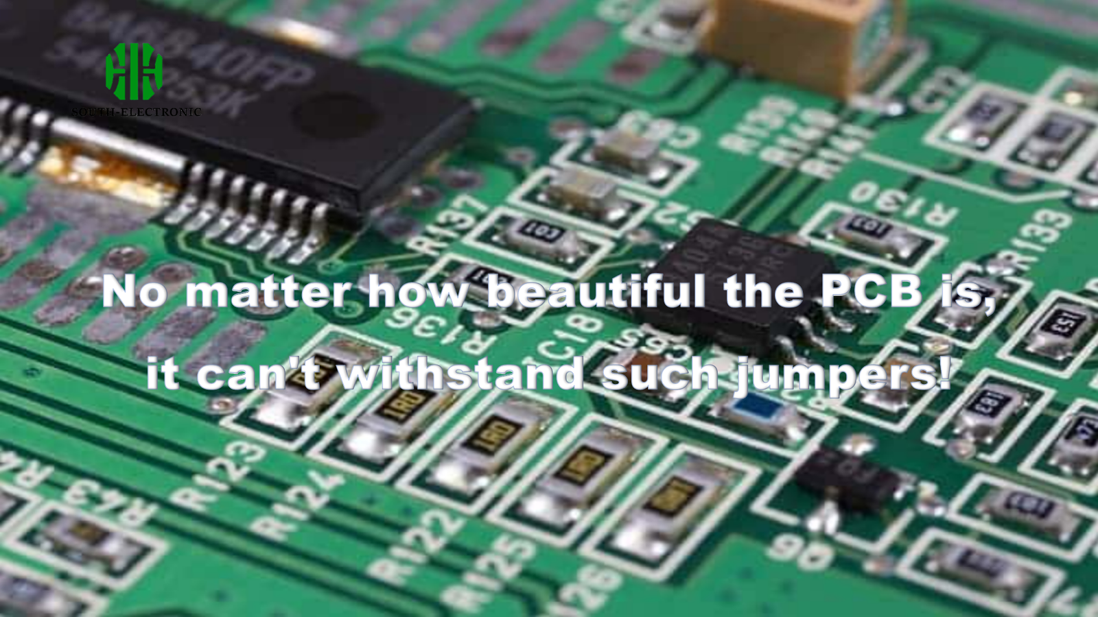
Learn to set up jumpers in single-sided PCBs using Altium Designer, including component configuration, jumper IDs, footprints, net assignments, and BOM integration for effective routing

Aluminum PCBs prevent overheating in high-power devices like LEDs and automotive systems through advanced thermal management and layered design.
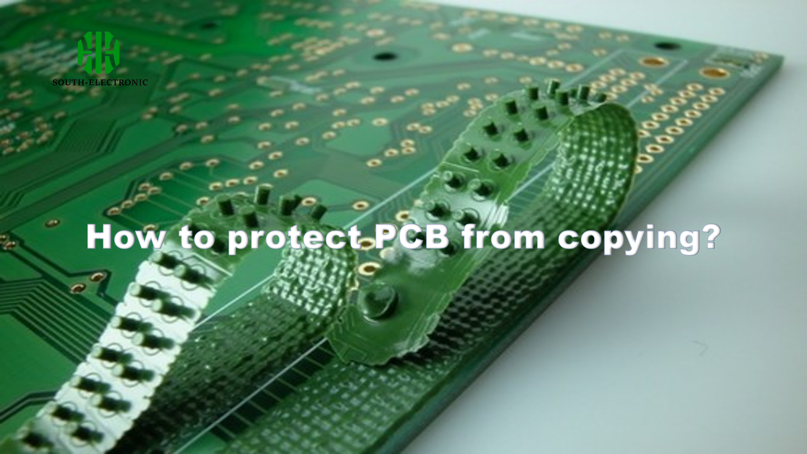
Stop PCB cloning with layered defense: encrypted firmware, anti-RE design tactics, legal shields, blockchain-tracked manufacturing.
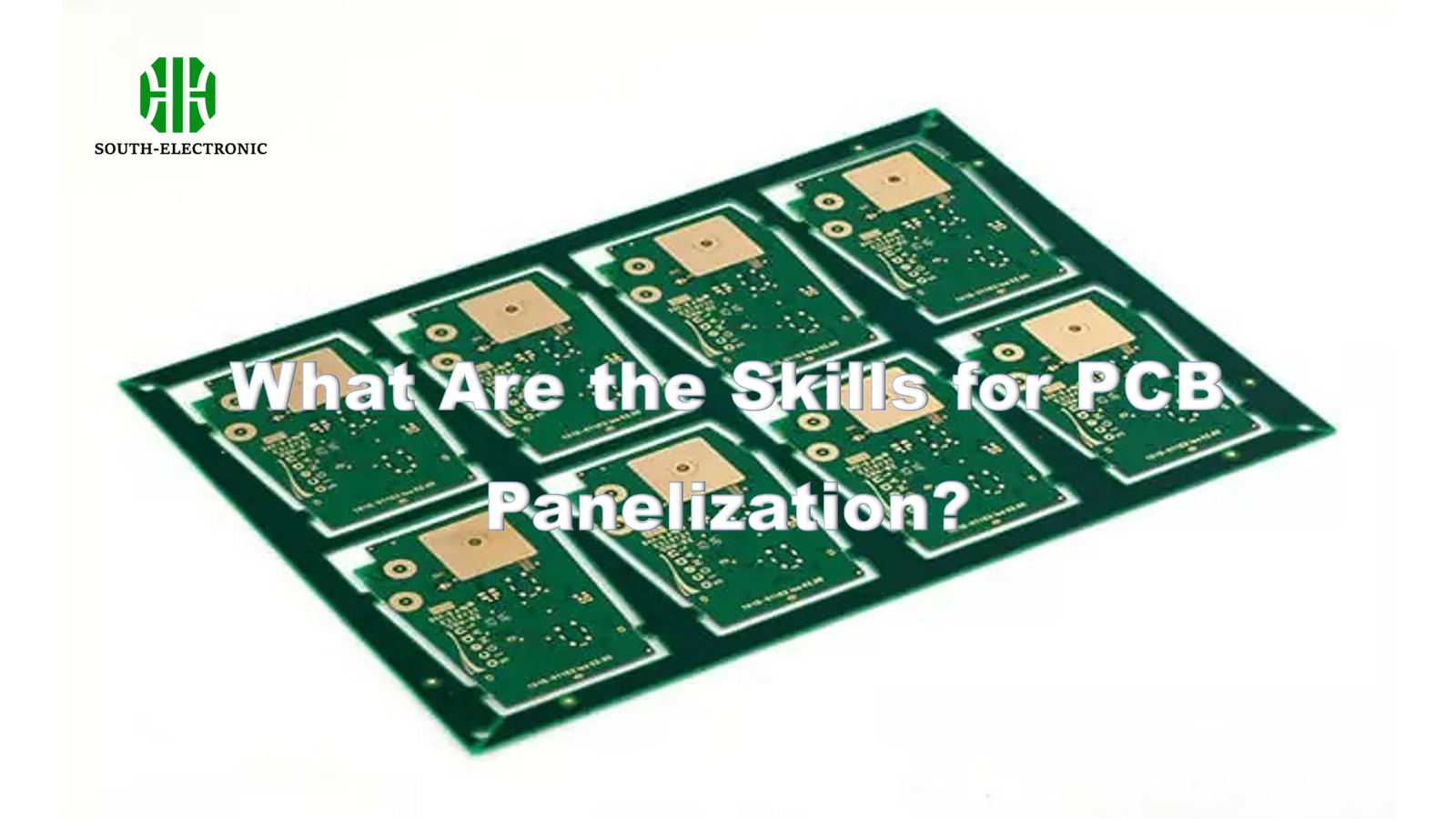
Master PCB panelization via V-scoring, tab routing, & layout optimization tools to boost efficiency and prevent production errors.
RF PCBs enable 5G, radar with low-loss materials (PTFE/Rogers), precise impedance control, and minimal signal distortion in high-frequency applications.

Effective PCB heat dissipation methods include thermal vias, copper cladding, strategic component layout, heatsinks, and airflow optimization to prevent hotspots.
Spot open vs short circuits: visual signs, safe repairs, smart prevention. Electrician insights to prevent fires and fix electrical issues.
IPC Class 2 vs Class 3: Key manufacturing standards, defect tolerances, industry uses, and cost differences for electronics reliability.
High voltage PCB design guide: material selection, creepage/clearance rules, insulation strategies, compliance standards, and testing methods for safety.