What’s the difference between immersion gold and gold plating on PCBs?
Gold plating (electrochemical process) creates thicker, harder surfaces ideal for durable applications like gold fingers. Immersion gold (chemical process) offers thinner, flatter finishes optimal for fine-pitch components and solderability.
What is the difference between PCB colors?
PCB color refers to solder resist layer hues like green, black, or red. Green dominates due to cost, contrast, military standards, and eco-friendliness. Other colors face trace visibility or production challenges.
What causes blistering on PCB surfaces?
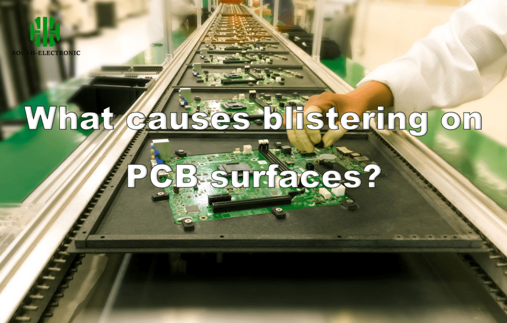
Key causes of PCB blistering: substrate issues, contamination, poor brushing, plating defects, microetching errors, oxidation, and process control failures.
Debugging a PCB: Five Essentially Foolproof Steps
Master PCB debugging with 5 essential steps: pre-power checks, safe power-on phases, structured troubleshooting, accurate measurement techniques, and fault isolation methods to prevent recurring issues.
Is your PCB pad design correct?
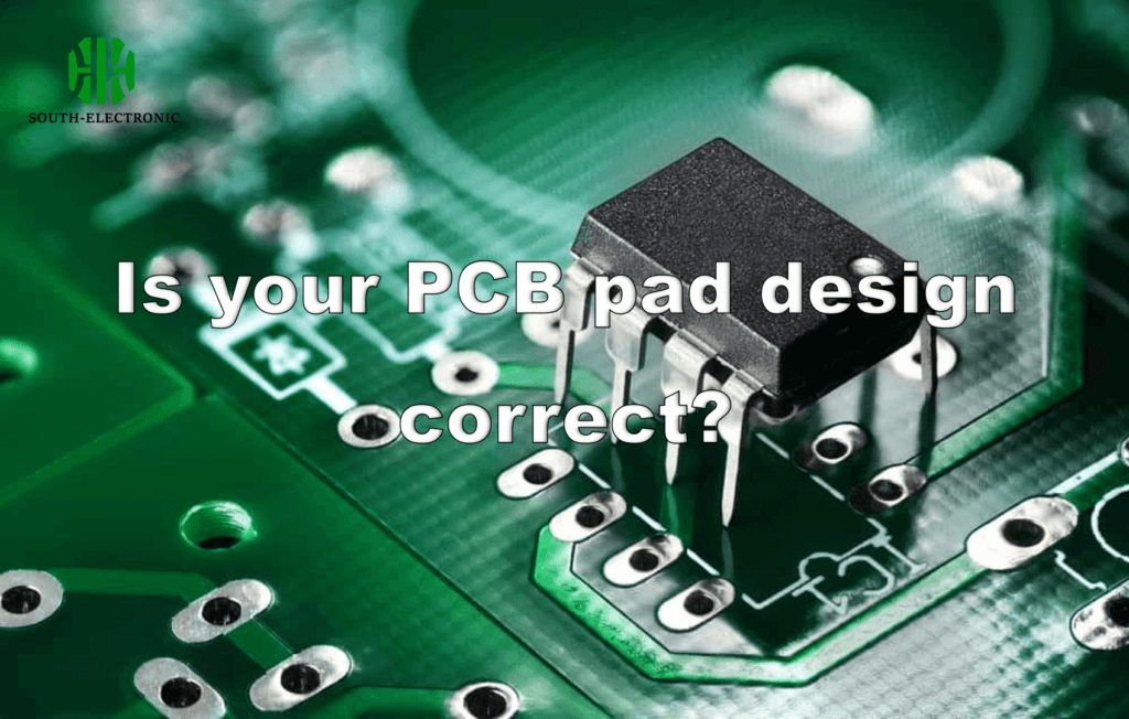
Proper PCB pad design is crucial for component reliability and manufacturability. Issues like solder bridging, tombstoning, and circuit breaks stem from incorrect pad sizing/placement. Standards guide SMT, BGA, and through-hole pad design.
A Complete Guide to Treating PCB Copper Surface Oxidation
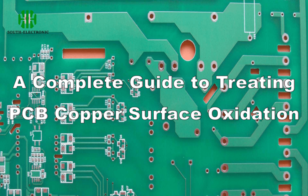
Combat PCB copper oxidation: explore causes (baking mishandling, coating loss, micro-pore humidity), treatment methods (cleaning, passivation, antioxidants), and prevention via storage/process optimization.
How to calculate PCBA assembly costs?
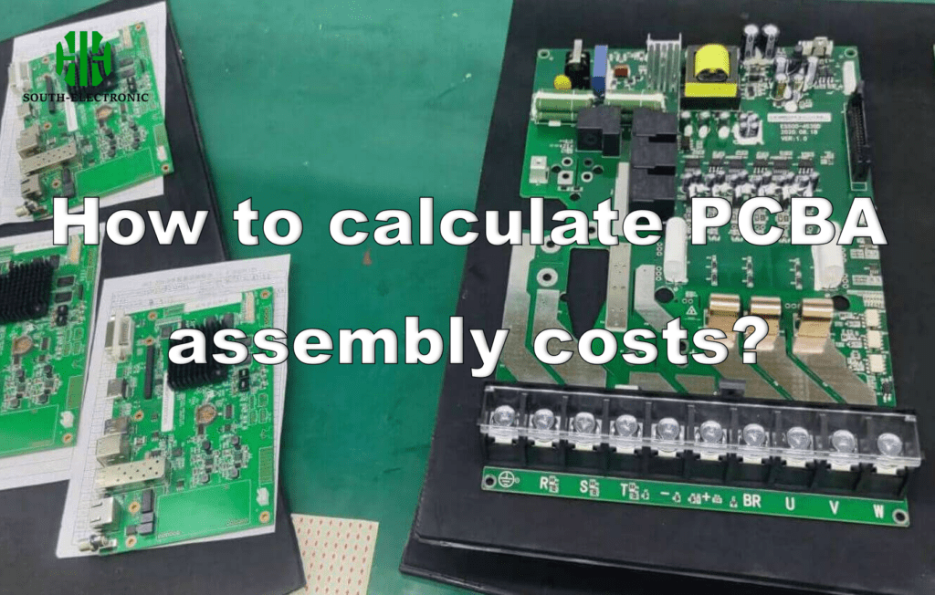
PCBA assembly costs include PCB fabrication fees (based on layers/material), component procurement (plus 5% loss), SMT processing (charged per component point), DIP assembly, testing, & other service fees.
A Comprehensive Guide to PCB Surface Treatment Processes
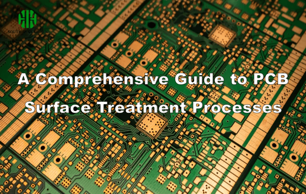
Learn why PCB surface treatment is essential to prevent copper oxidation and ensure reliability. Explore HASL, OSP, ENIG, Immersion Silver, Tin processes. Choose based on cost, application, environment, solderability, and storage.
What is PCB solder mask?
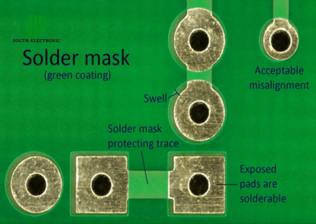
Learn the 4 types of PCB solder mask: Top/Bottom, Epoxy Liquid, Liquid Photoimageable (LPI), and Dry Film. Compare applications, design rules, and thickness for optimal rust/short prevention.
How many PCB testing methods do you know?
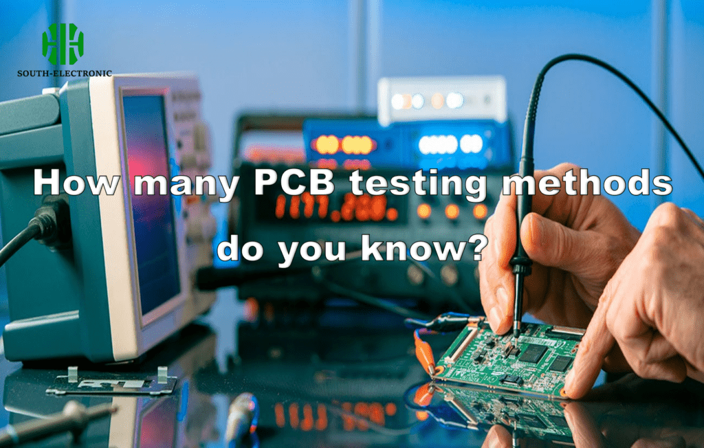
Explore 13 vital PCB testing methods (ICT, Flying Probe, AOI, X-ray, etc.) ensuring reliability & preventing defects in electronic manufacturing. Critical for quality control.