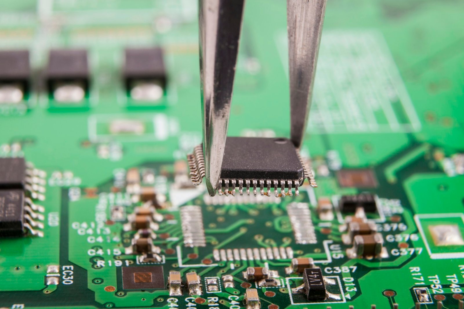
Master PCB Stackup Design Tips in One Article
Learn PCB stackup design principles (adjacent ground layers, symmetry) for optimal impedance matching in high-speed circuits. Includes RK3588 8-layer through-hole case study with trace width calculations using DFM tools.
What are the causes of uneven color in PCB manufacturing?
Learn 11 causes of uneven PCB color like squeegee blade issues, improper ink viscosity, screen gap problems & printing speed. Discover fixes for consistent PCB appearance.
How to standardize the design of ceramic PCB substrates?
Design specs for Al₂O₃, AlN, Si₃N₄ ceramic substrates. Covers HTCC/LTCC/DPC processes, electrical/thermal/mechanical design, reliability requirements, and material selection for power/RF/LED applications.
The Most Comprehensive SMT Reflow Process Analysis Ever
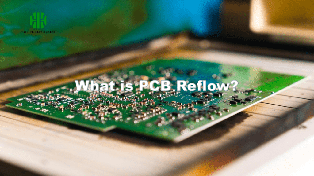
Comprehensive guide to 9 reflow soldering types: hot plate, IR, IR+hot air, nitrogen, double-sided, through-hole, lead-free, flex board & vertical vacuum ovens. Compares mechanisms, benefits & SMT applications.
How important are Gerber files in PCB manufacturing?
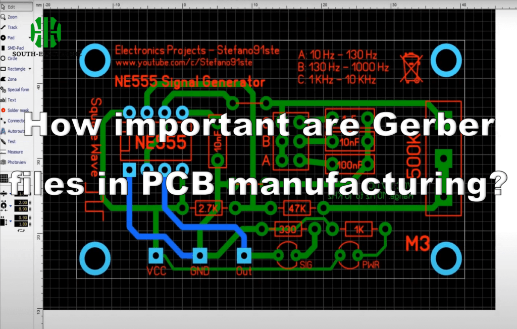
Gerber files are standardized PCB design formats critical for manufacturing. They define layers, dimensions, and components to prevent errors, reduce costs, and ensure efficient production. Latest version: Gerber X2.
What are the causes of poor PCB etching?

PCB etching defects like undercutting, interlayer shorts, over-etching, and resist erosion critically impact yield & reliability. Strict control & maintenance are vital.
What are the circuit board parameters?
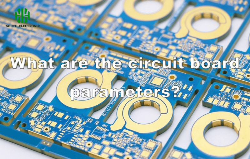
Master PCB design by optimizing material standards, high Tg for thermal endurance, and high-frequency specs like Dk/Df. Prevent signal loss, warping, and failures in reliable electronics.
What is an HDI board?
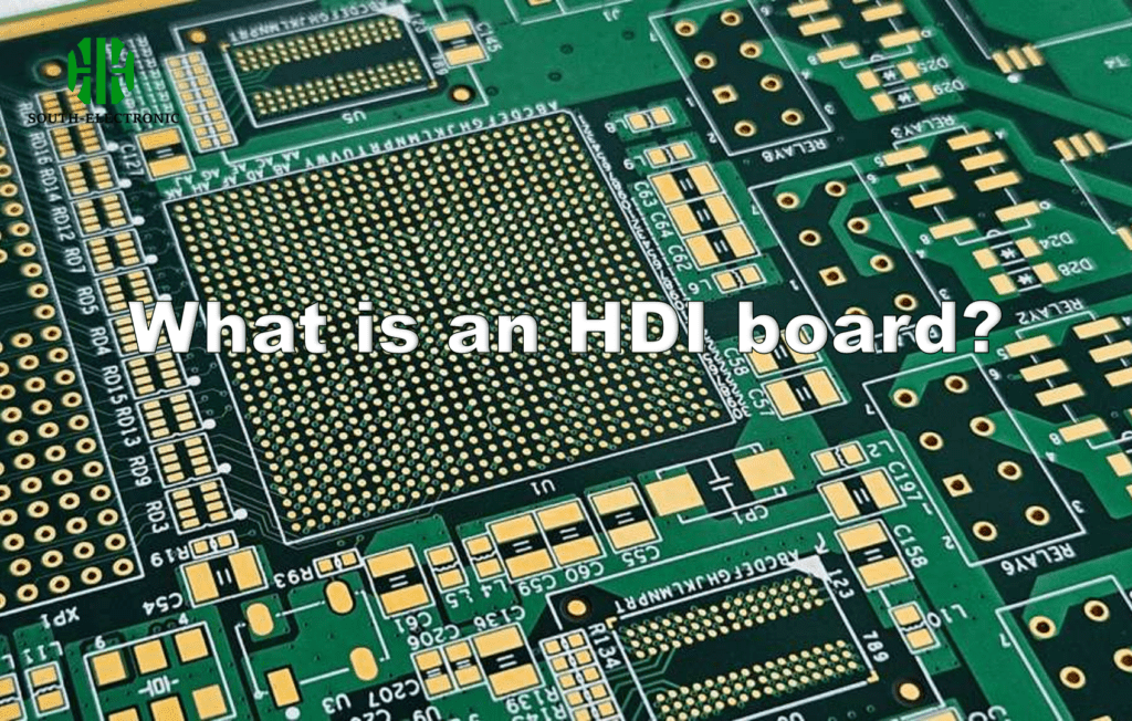
HDI PCBs pack micro-vias ≤150μm and conductor spacing ≤100μm for ultra-high density. They outperform standard PCBs in wiring density, thermal dissipation, and signal integrity across orders.
How can you give a damaged PCB a new lease of life?

Learn 8 practical PCB pad repair techniques like copper foil, epoxy fills & trace jumpers. Save damaged boards from scrap with Jiepei’s professional rework methods. Reliable solutions explained!
How to optimize PCB design to reduce short circuits?

Prevent PCB shorts & opens: ensure trace/via clearance, proper pad spacing, control impedance, minimize vias, optimize power/ground, prioritize testability & DFM standards.