

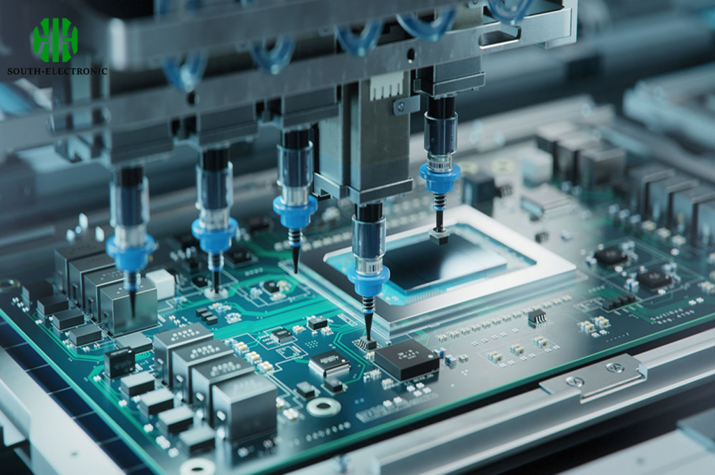
Faulty circuit boards ruin products and reputations. Imagine shipping defective gadgets to customers – costly recalls follow instantly. Prevent disasters by using proven testing techniques!
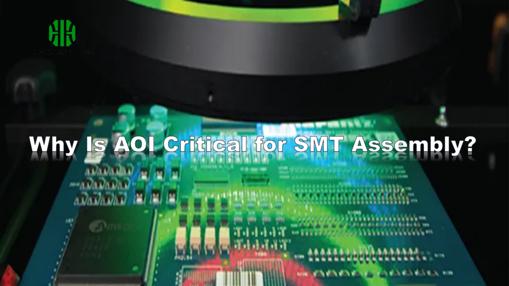
Automated Optical Inspection (AOI), In-Circuit Testing (ICT), Flying Probe Testing, and Functional Testing are the most common PCBA checks. Others like X-ray and Burn-in testing add crucial reliability layers, catching failures before products ship.
Choosing the right methods saves money and prevents headaches. Let’s break down how each technique protects your electronics.
How to choose the right PCBA testing strategy: ICT, FCT, or AOI?
PCB failures cost thousands per hour on production lines. Picking wrong tests means missing hidden flaws. Match methods to your real needs!
ICT checks component values and connections electrically. FCT validates full product functionality like real users. AOI scans for visible defects like soldering issues. Combine them based on complexity.
Picking your inspection toolkit
Three factors decide your testing mix: budget, volume, and risk level.
| Test coverage tradeoffs | Method | Defects Caught | Cost | Speed |
|---|---|---|---|---|
| AOI | Solder bridges, missing parts | Low | Fast (seconds) | |
| ICT | Wrong components, opens/shorts | High | Medium | |
| FCT | Software bugs, power issues | Very High | Slow |
Small batches suit Flying Probe and AOI – no custom fixtures needed. High-volume lines need ICT’s speed. Medical or automotive gear? Always add FCT for safety checks. One factory skipped FCT for cost; 30% of their smart thermostats overheated in homes. Balance your risks: minor toys need basic scans, life-saving devices demand full validation.
Start with AOI for surface defects, then add electrical checks if failure costs exceed test expenses.
How does PCBA testing save money?
Catching one failed board post-assembly costs 10x more than early detection. Recall expenses can bankrupt small firms. Testing is insurance against catastrophic waste!
Early fault discovery slashes rework labor and scrap rates. A $2 AOI scan prevents $50 recalls. Consistent testing also reduces warranty claims over product lifetimes.

The failure cost waterfall
Three financial pits swallow profits without testing:
| 1. Manufacturing loss stages | Stage | Cost Multiplier | Common Issues Caught |
|---|---|---|---|
| Component | 1x | Counterfeit parts | |
| Assembly | 5x | Cold solder joints | |
| Final Product | 20x | Intermittent faults |
My first prototype missed Burn-in testing – field failures required 200 replacements. X-ray inspection later found weak solder under chips.
2. Brand damage ripple effect
One viral social media post about malfunctioning gadgets scares away future buyers. Testing maintains reputation capital.
3. Continuous feedback benefits
Test data reveals chronic issues like bad capacitor batches. Fixing root causes lifts overall yield rates permanently, turning testing from expense to profit generator.
What to do when PCBA testing fails?
Failed tests paralyze production lines. Panic causes rash decisions – like skipping retests. Systematically diagnose instead of guessing!
First, isolate failure patterns. Cluster errors by test type, location, or component. Then cross-check with manufacturing data like solder paste dates. Finally, validate fixes with targeted retests.

Structured debug framework
Fix failures faster with these steps:
| Failure response priorities | Step | Action | Tool Examples | Time Goal |
|---|---|---|---|---|
| 1 | Replicate failure | Thermal camera, scope | <1 hour | |
| 2 | Trace root cause | X-ray, cross-sections | 1-4 hours | |
| 3 | Develop corrective action | Soldering rework | 8 hours |
When our AOI flagged solder voids, X-rays showed inconsistent paste thickness. Stencil cleaning fixed 80% of defects.
Escalation thresholds
- Single board failure: Rework individually
- 5% batch failure: Stop line, check recent process changes
- 10%+ failure: Halt shipments, audit entire build workflow
Document every solved case in a defect library. This turns failures into future prevention guides. Always update tests to catch similar flaws earlier next time!
Conclusion
PCBA testing isn’t optional – AOI, ICT, and FCT are core shields against costly defects. Choose methods matching your risks, act systematically on failures, and watch savings accumulate yearly.

