What is PCBA?
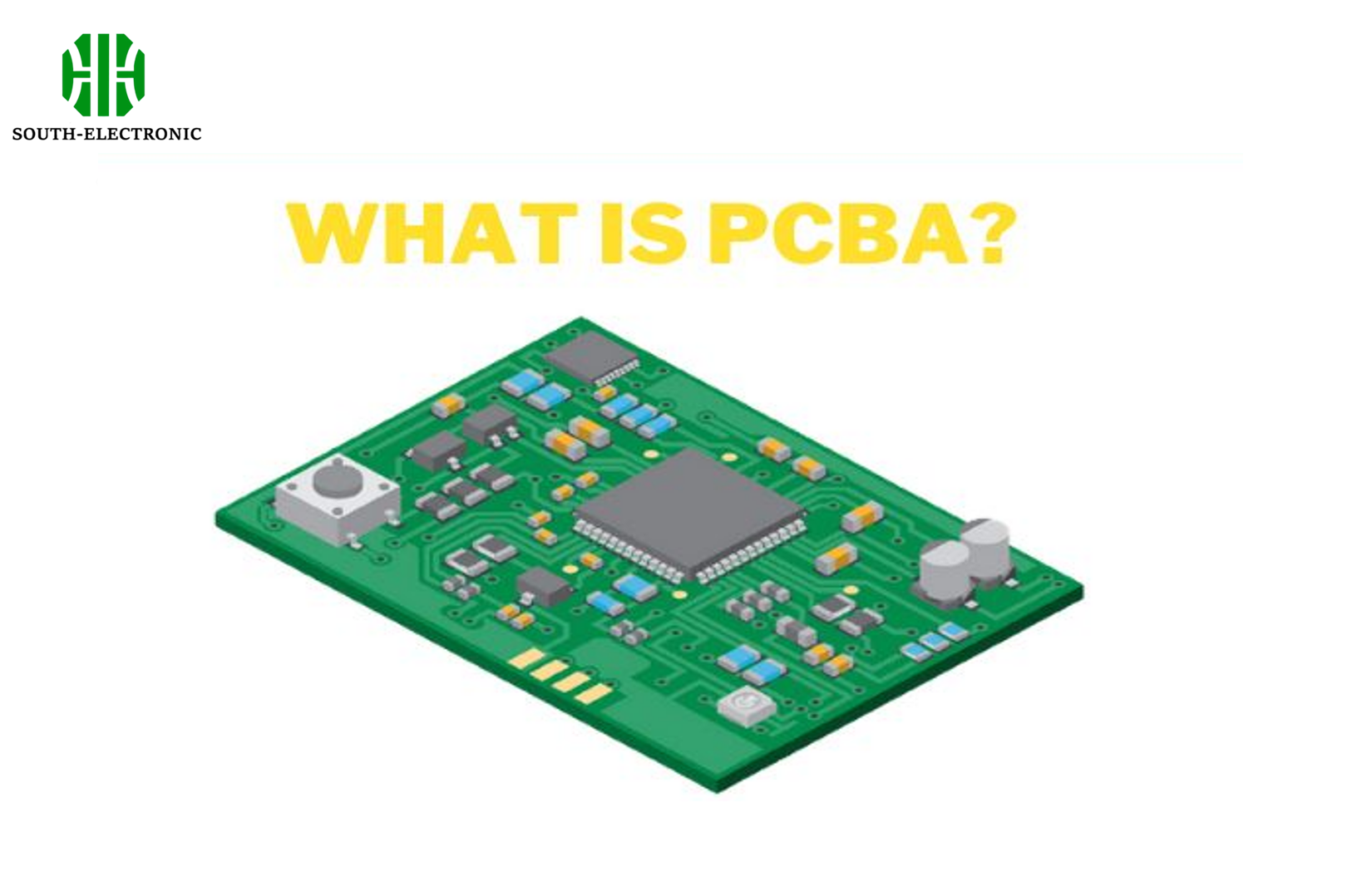
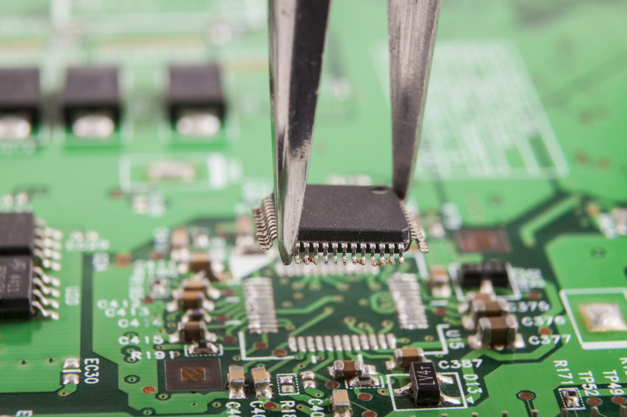
Printed Circuit Board Assembly (PCBA) refers to the process of soldering or assembly of electronic components to a printed circuit board (PCB). A PCB is a blank circuit board with no components installed. Once the electronic components are soldered onto the PCB, it becomes a PCBA. This process is essential in creating functional electronics for various applications.
Difference between PCBA and PCB
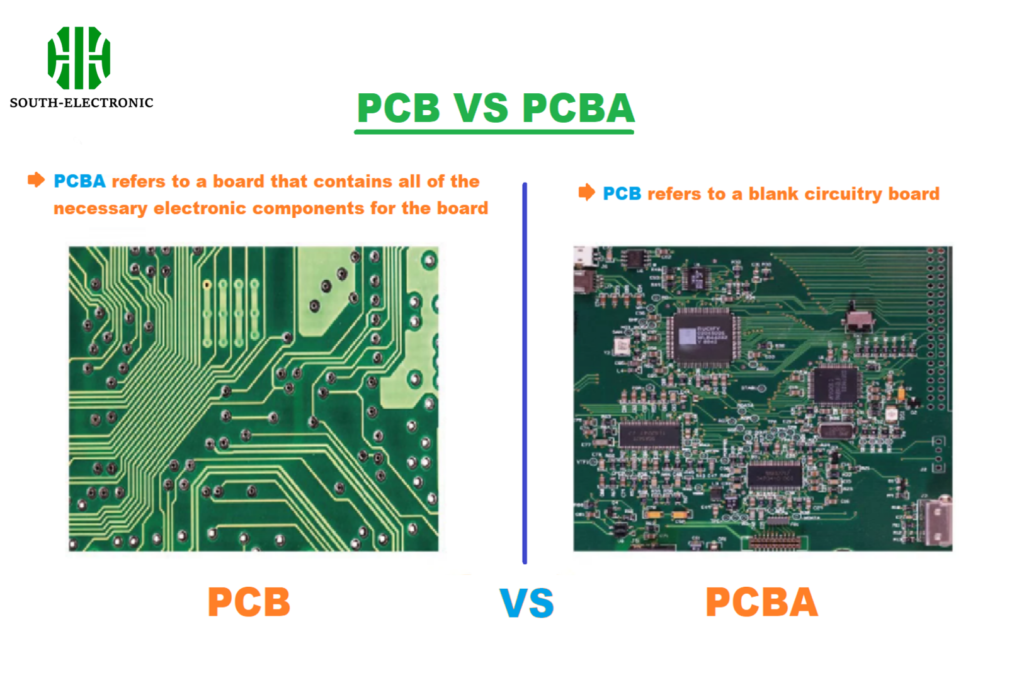
PCB (Printed Circuit Board): A PCB refers to a board made from non-conductive materials with conductive paths, pads, and other features etched from copper sheets to connect different components. It serves as the foundation that supports and wires the surface-mounted and socketed components in most electronics.
PCBA (Printed Circuit Board Assembly): PCBA refers to a PCB that has been assembled with electronic components, making it a functional printed circuit assembly or board. The process involves soldering electronic components to a PCB and testing it to ensure functionality.
Types of PCBA Technologies
PCBA technologies can primarily be classified into three types:
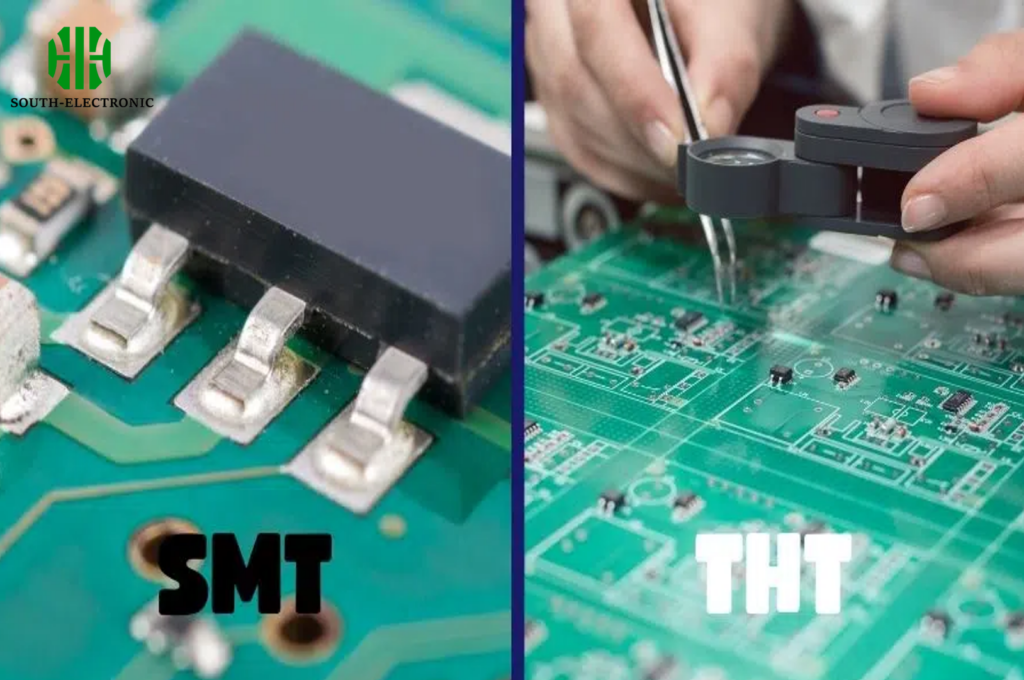
- Through-Hole Technology (THT): Components have leads inserted into holes drilled in the PCB and are soldered to pads on the opposite side. This method is favored for its strong mechanical bonds.
- Surface-Mount Technology (SMT): Components are mounted directly onto the surface of a PCB. SMT has become more prevalent due to its ability to accommodate a larger number of smaller components and its easier automation, speeding up the assembly process.
- Mixed Technology: This involves using both THT and SMT on the same PCB. This approach is used to optimize the benefits of both technologies based on the application’s specific needs.
Steps Involved in PCBA Manufacturing Process
The PCBA manufacturing process typically includes the following steps:
- Solder Paste Stenciling: Apply solder paste to the PCB where components will be placed.
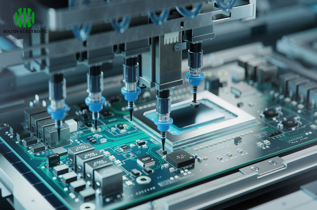
- Pick and Place: Robots place surface-mount components on the PCB.
- Reflow Soldering: The PCB passes through a reflow oven to melt the solder paste and form connections between components and the board.
- Inspection and Quality Control: This may involve manual checks, automatic optical inspection, and X-ray inspection to verify soldering quality and component placement.
- Through-Hole Component Insertion: For boards using THT, components are placed and soldered.
- Final Inspection and Functional Test: The completed board is tested to ensure it meets the required specifications.
Common Testing Methods:
| Testing Method | Description |
|---|---|
| Visual Inspection | Checking for visible defects and proper assembly |
| In-Circuit Testing | Testing individual components on the board |
| Functional Testing | Verifying the overall functionality of the PCBA |
Uses and Applications of PCBA
PCBAs are used in virtually every electronic device. Some common applications include:
- Consumer Electronics: Smartphones, computers, televisions, and home appliances.
- Medical Equipment: Diagnostic and monitoring devices.
- Automotive Components: Engine control units, infotainment systems.
- Industrial Machinery: Sensors and automation equipment.
- Telecommunications: Routers, switches.
PCBAs are super important for making sure electronic devices work right and don’t break. They’re like the roads that let power and signals go between all the parts in a device. At South-Electronic, we do everything you need to make a PCBA, from designing it to putting it together, and we even get all the parts and test it for you. We make it easy for you to get a PCBA that works right. Get in touch with us and we’ll help you get started on your PCBA project right now!

