
What Is PCB Via Tenting?
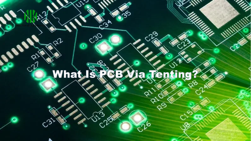
Tented vias prevent solder shorts but impact thermal/EM performance. Choose based on environmental needs vs. signal speed requirements.
What should I pay attention to in DFM check?
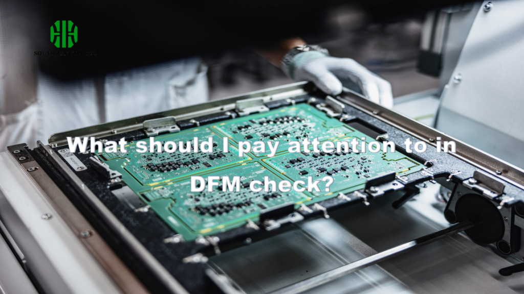
Prevent PCB errors via DFM checks: validate design rules, component placement, materials, stackup symmetry for cost-efficient manufacturing.
How to Optimize High Current PCB for Motor Controls?
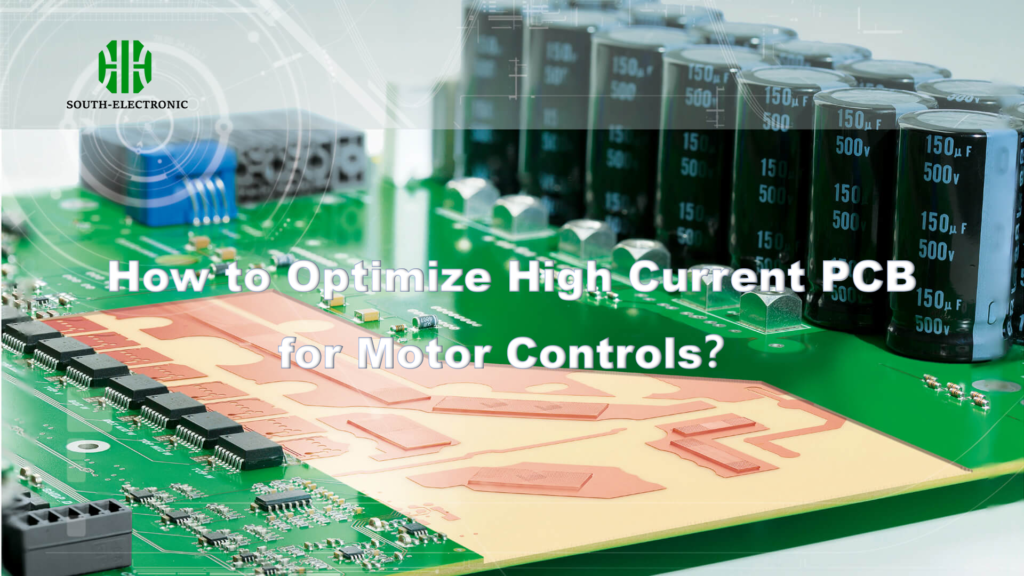
Optimize high-current motor PCBs with strategic copper weights, IPC-2152 traces, cross-ply laminates, and Kelvin sensing for 60% thermal stress reduction.
How to Prevent PCB Delamination?
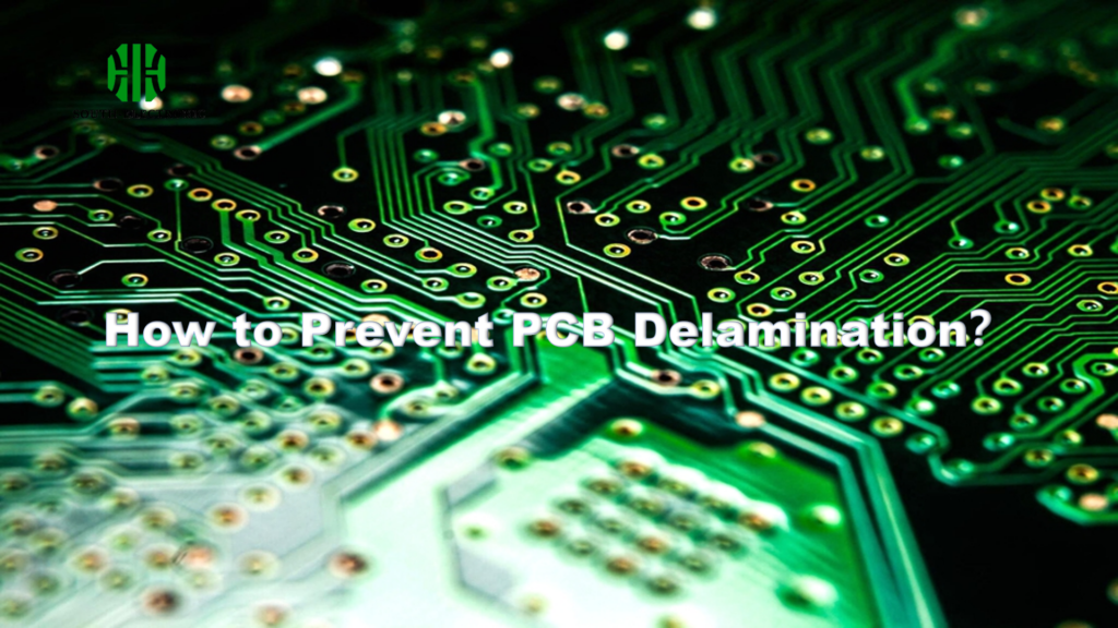
Prevent PCB delamination by controlling moisture exposure, selecting high-Tg materials, optimizing thermal processes, and balancing copper distribution.
Meta Description (110 characters):
Learn moisture control, material selection, and process optimization strategies to prevent PCB delamination in manufacturing.
Keywords:
PCB delamination prevention, moisture control in PCBs, high Tg PCB materials, CTE mismatch solutions, thermal shock prevention, lamination pressure parameters, FR-4 alternatives, PCB material selection guide, copper balancing design, PCB assembly process controls, thermal stress reduction, moisture sensitivity levels (MSL), TGA testing for PCBs, PCB reliability improvement, PCB layer separation causes.
