
What is a Via in PCB Design?

Master PCB via design: Choose blind/buried vias for dense layouts, calculate size/spacing to prevent overheating, and avoid common failure causes. Essential for modern circuit reliability.
How to Read Schematic Diagram?
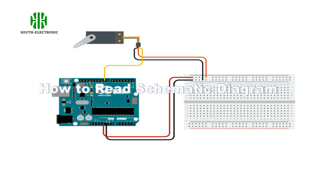
Learn circuit schematic basics: wire connection rules (dots = connected), component symbols like Rs and Cs, and practical debugging steps using diagrams to avoid wiring disasters.
What Are the Key Advantages and Disadvantages of BGA Packages?

Master BGA packages: superior density & thermal performance need precision soldering, X-ray inspection, and BGA vs LGA comparison for optimal electronics assembly reliability.
