What are the rules for 8-Layer PCB Stackup ?
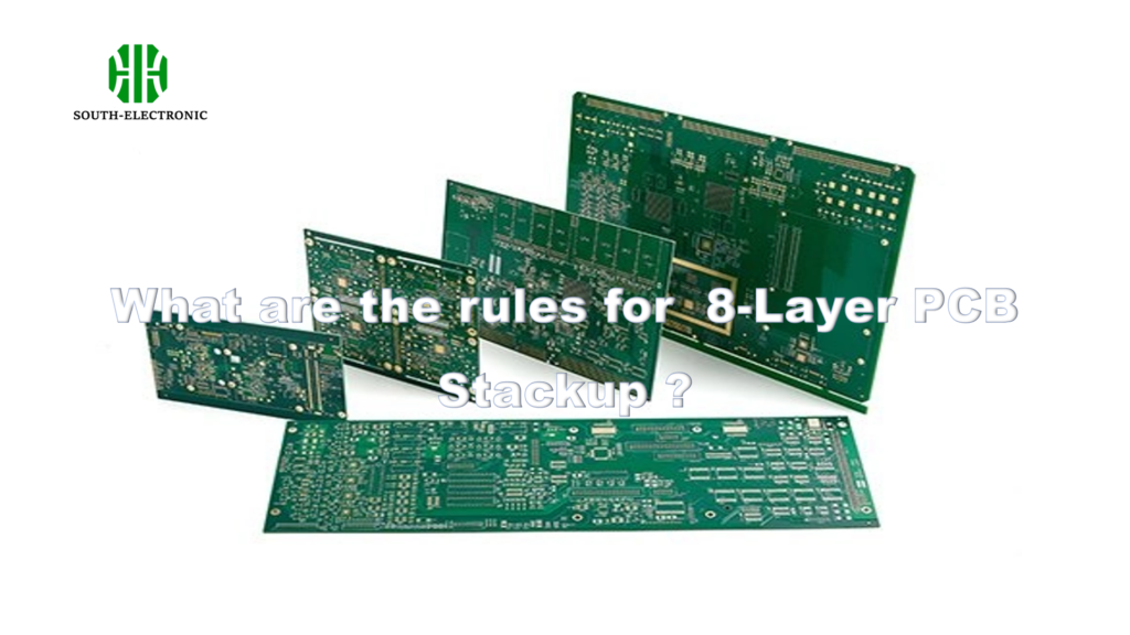
Master 8-layer PCB stackups: Optimize configurations for high-speed/mixed signals. Precisely calculate impedance and thickness. Cut costs by 30% with material and design hacks.

How to Start Your First PCB Design?
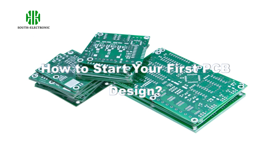
Free step-by-step PCB design guide for beginners: Learn software selection, avoid fatal layout errors, and prepare manufacturing files correctly to save time & money.

Get in touch

Where Are We?

Factory Address

Industrial Park, No. 438, Shajing Donghuan Road, Bao'an District, Shenzhen, Guangdong, China

Head Office Address

Floor 4, Zhihui Creative Building, No.2005 Xihuan Road, Shajing, Baoan District, Shenzhen, China

HK Office Address

ROOM A1-13,FLOOR 3,YEE LIM INDUSTRIAL CENTRE 2-28 KWAI LOK STREET, KWAI CHUNG HK,CHINA

Let's Talk

Phone : +86 400 878 3488

Send Us A Message

The more detailed you fill out, the faster we can move to the next step.

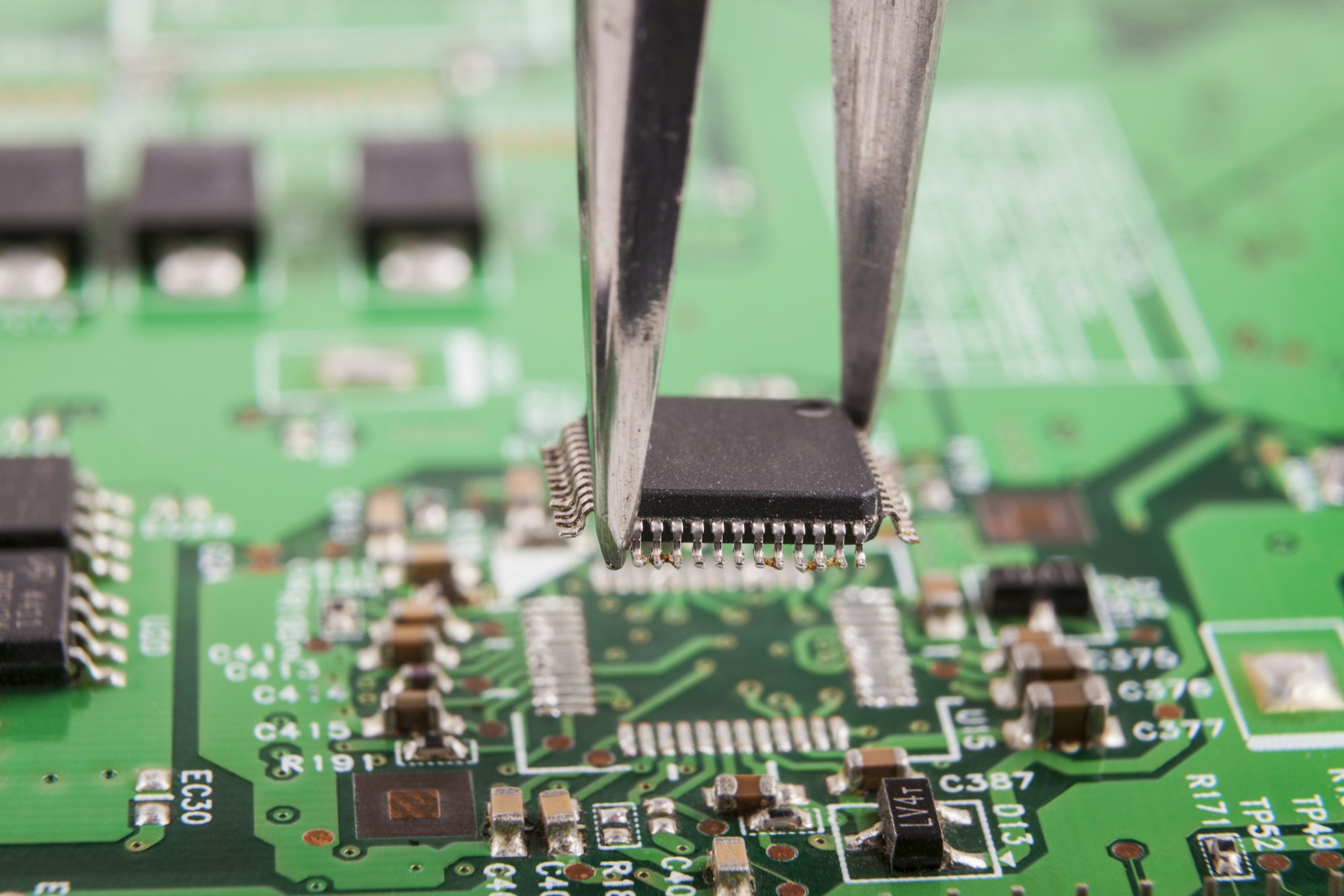
Microchip Removal