
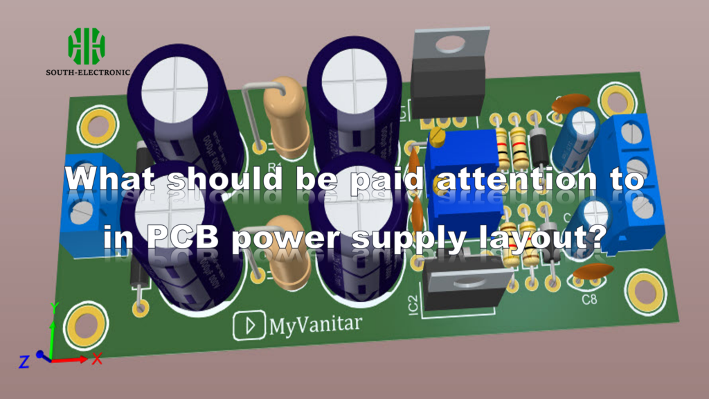
What should be paid attention to in PCB power supply layout?
Critical PCB layout practices for buck converters: minimize high-di/dt power loop area with short/thick traces, place input caps near Vin/PGND, reduce SW noise impact, and optimize copper/vias for thermal/EMI performance. Essential for stable power delivery.
How to Design the Perfect BGA?

Master BGA design: Avoid routing nightmares, thermal chaos & hidden defects with IPC standards, microvia strategies, thermal management, rework, and advanced QA.
