What is a blind via?

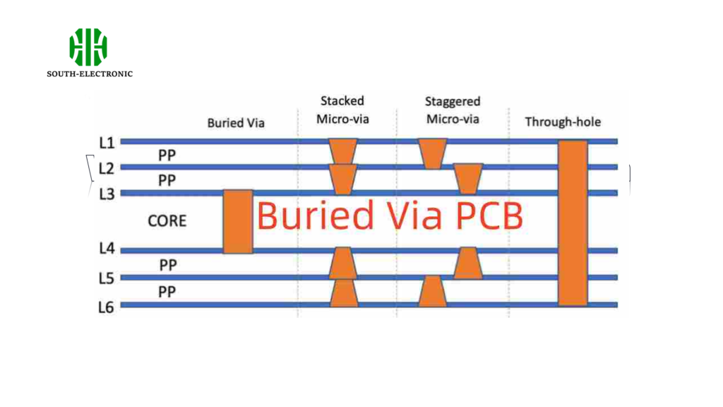
Blind vias save space in dense PCBs by connecting outer to inner layers selectively. Essential for HDI designs like smartphones, they optimize routing & thermal management, but increase cost 15-30%. Combines with microvias.

What are the most common PCBA testing methods?

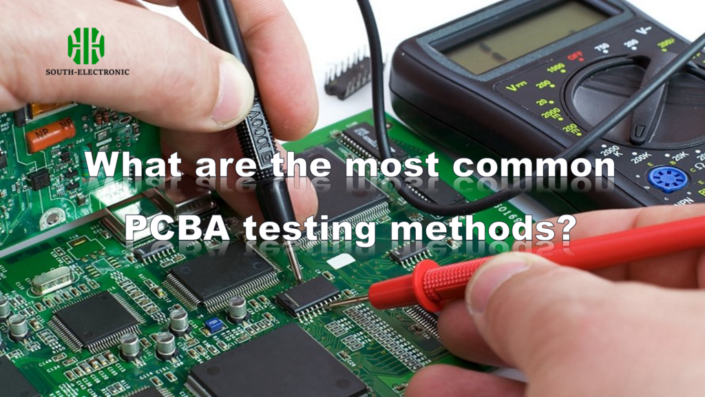
PCBA testing (AOI, ICT, FCT) catches defects early, prevents recalls & saves costs. Choose methods by risk, budget & volume. Systematically debug failures to protect reputation & profits.

Get in touch

Where Are We?

Factory Address

Industrial Park, No. 438, Shajing Donghuan Road, Bao'an District, Shenzhen, Guangdong, China

Head Office Address

Floor 4, Zhihui Creative Building, No.2005 Xihuan Road, Shajing, Baoan District, Shenzhen, China

HK Office Address

ROOM A1-13,FLOOR 3,YEE LIM INDUSTRIAL CENTRE 2-28 KWAI LOK STREET, KWAI CHUNG HK,CHINA

Let's Talk

Phone : +86 400 878 3488

Send Us A Message

The more detailed you fill out, the faster we can move to the next step.

Microchip Removal