How to test bare PCB board?

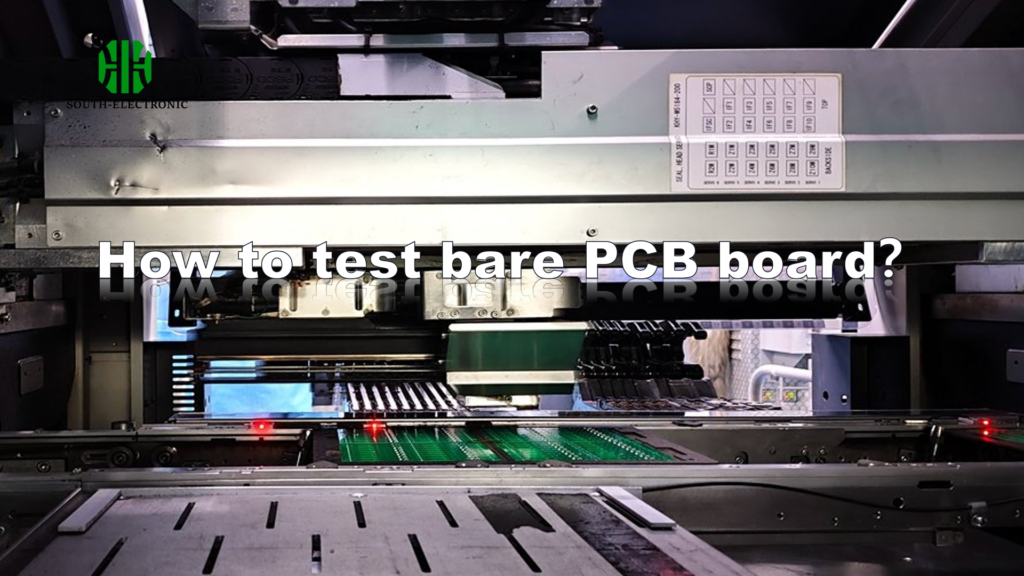
Test bare PCBs with flying probe, AOI, and impedance meters to catch hidden flaws early. Balance materials, tolerances, and layer count to control costs and prevent assembly failures.

What is PCB via stitching?

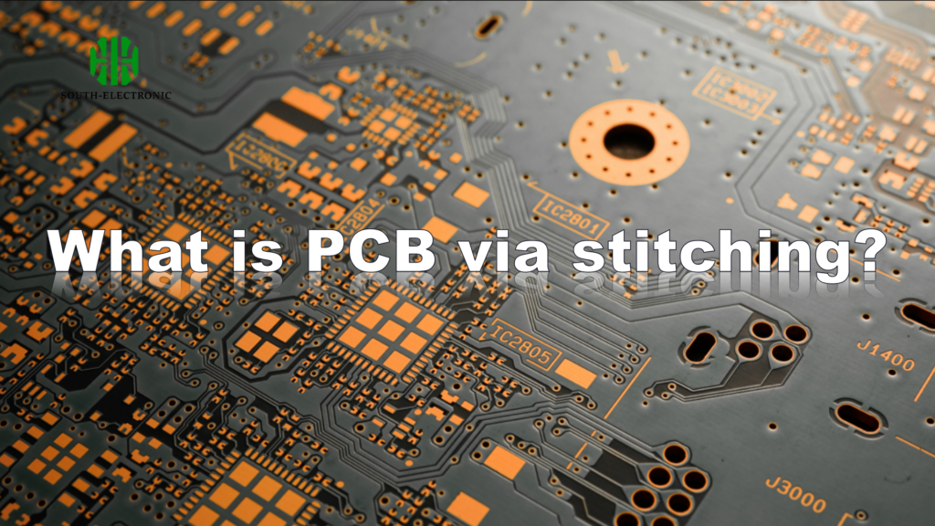
PCB via stitching creates parallel return paths to suppress EMI and boost signal integrity in high-speed designs, but overuse risks PCB fractures during manufacturing—balance is key.

Get in touch

Where Are We?

Factory Address

Industrial Park, No. 438, Shajing Donghuan Road, Bao'an District, Shenzhen, Guangdong, China

Head Office Address

Floor 4, Zhihui Creative Building, No.2005 Xihuan Road, Shajing, Baoan District, Shenzhen, China

HK Office Address

ROOM A1-13,FLOOR 3,YEE LIM INDUSTRIAL CENTRE 2-28 KWAI LOK STREET, KWAI CHUNG HK,CHINA

Let's Talk

Phone : +86 400 878 3488

Send Us A Message

The more detailed you fill out, the faster we can move to the next step.

Microchip Removal