What is the standard size of a PCB panel?

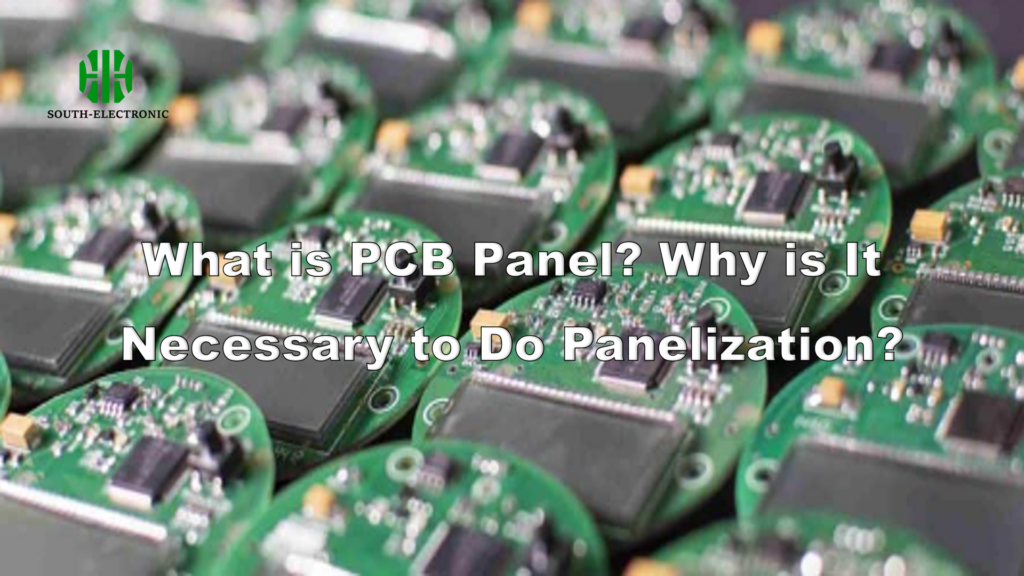
Optimize standard PCB panel sizes (18×24″, 12×18″) to cut costs. Choose breakaway methods wisely, minimize material waste, and avoid design errors to maximize yield and profit.

What is the potting process in PCB?

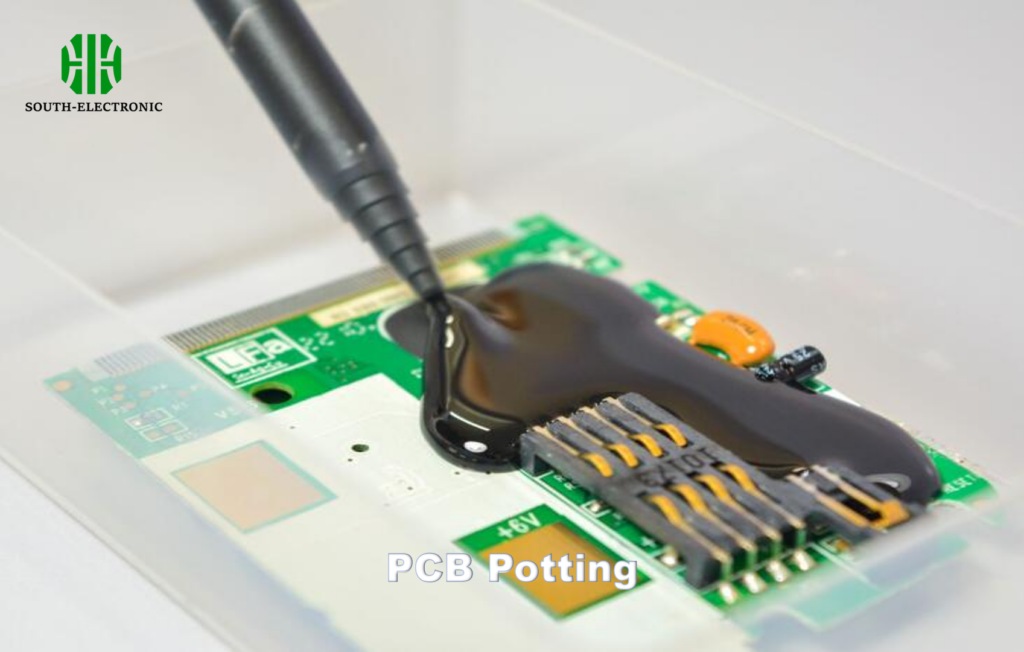
PCB potting seals assemblies in resin for extreme environment protection. Learn potting vs. conformal coating selection, process tips to prevent voids/cracks, and avoid hidden costs. Essential for harsh applications.

Get in touch

Where Are We?

Factory Address

Industrial Park, No. 438, Shajing Donghuan Road, Bao'an District, Shenzhen, Guangdong, China

Head Office Address

Floor 4, Zhihui Creative Building, No.2005 Xihuan Road, Shajing, Baoan District, Shenzhen, China

HK Office Address

ROOM A1-13,FLOOR 3,YEE LIM INDUSTRIAL CENTRE 2-28 KWAI LOK STREET, KWAI CHUNG HK,CHINA

Let's Talk

Phone : +86 400 878 3488

Send Us A Message

The more detailed you fill out, the faster we can move to the next step.

Microchip Removal