
Blind, Buried, or Through Via?
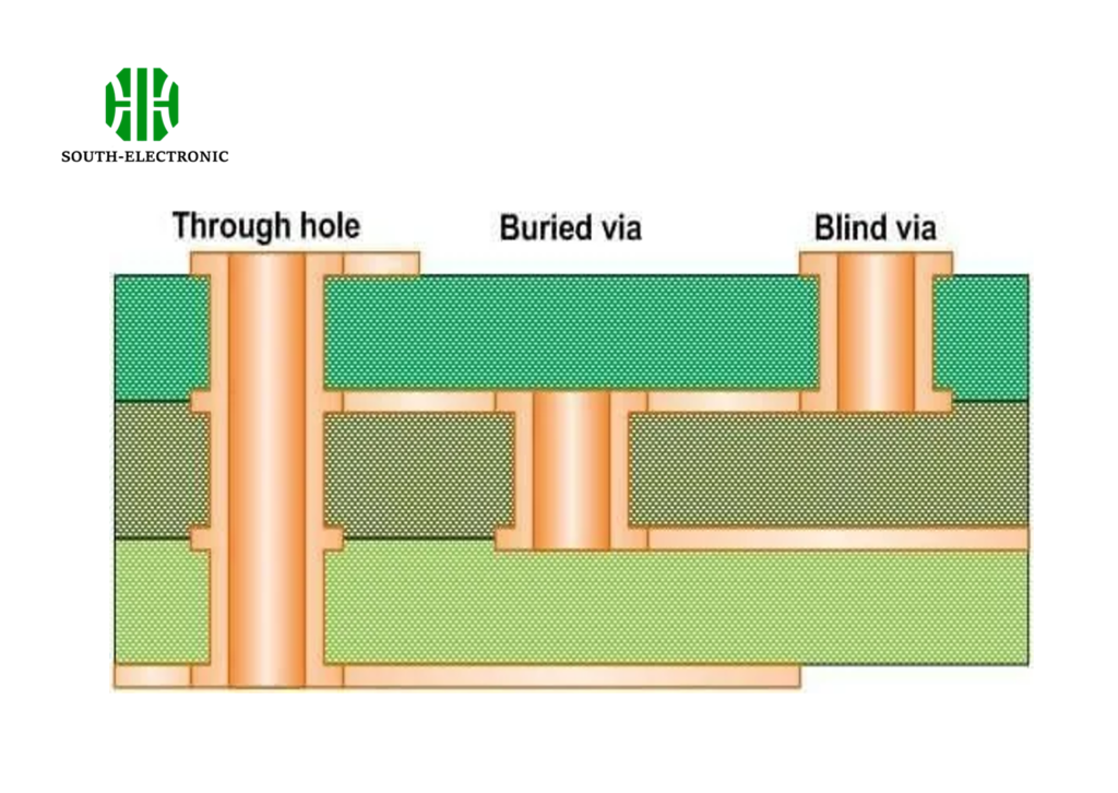
Master PCB via selection: balance cost, density & signal needs. Proper sizing prevents overheating. Understand via-pad differences. Prevent failures with plating standards.
Is Your FR-4 Board Right for High-Speed Signals?
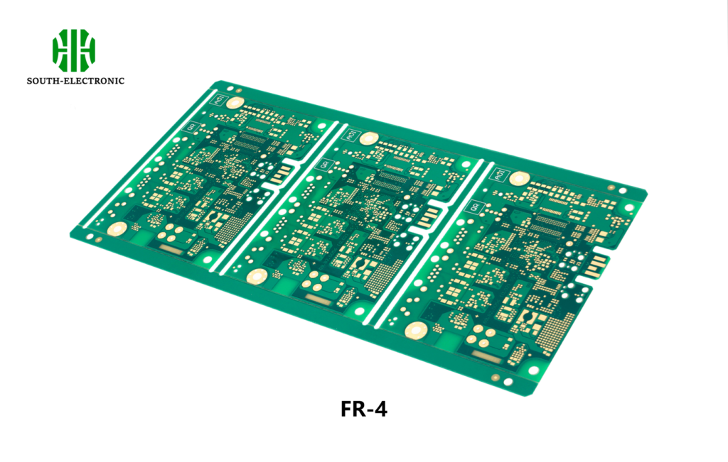
FR-4 supports MHz designs affordably but suffers dielectric losses >5GHz/long traces. Optimize layer stackup, thermal design & shielding – or switch to low-loss laminates for GHz needs.
