
Is your PCB pad design correct?
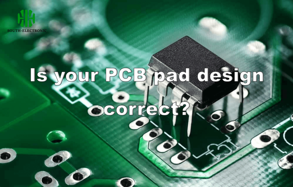
Proper PCB pad design is crucial for component reliability and manufacturability. Issues like solder bridging, tombstoning, and circuit breaks stem from incorrect pad sizing/placement. Standards guide SMT, BGA, and through-hole pad design.
A Complete Guide to Treating PCB Copper Surface Oxidation
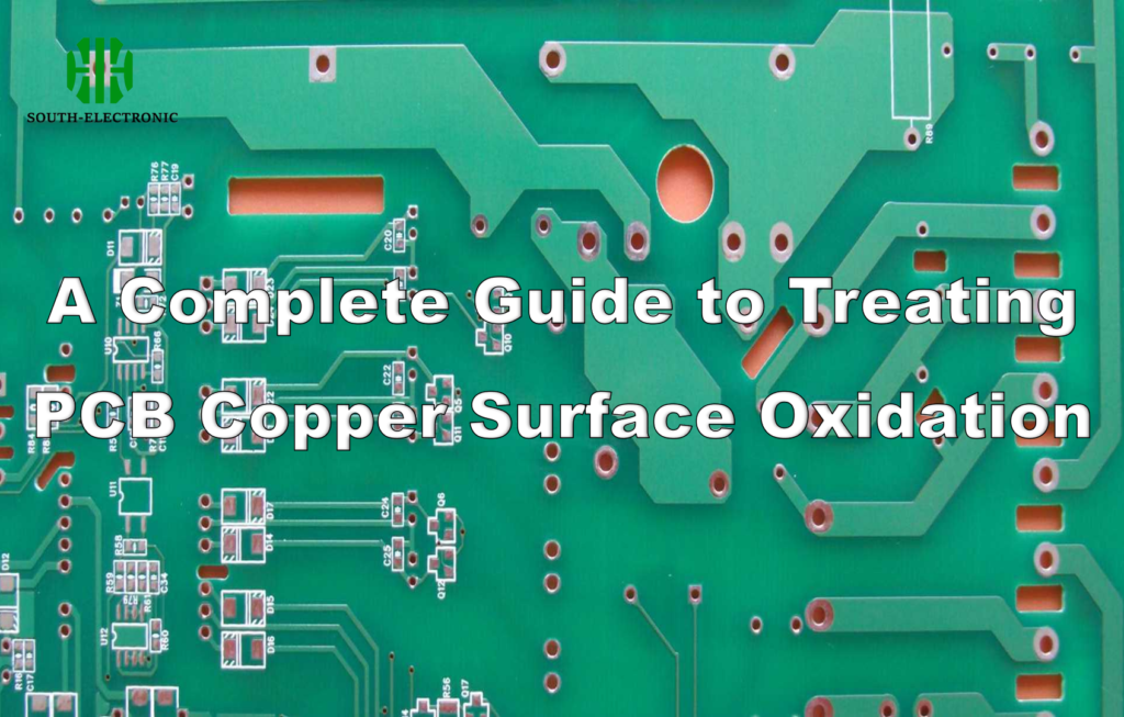
Combat PCB copper oxidation: explore causes (baking mishandling, coating loss, micro-pore humidity), treatment methods (cleaning, passivation, antioxidants), and prevention via storage/process optimization.
