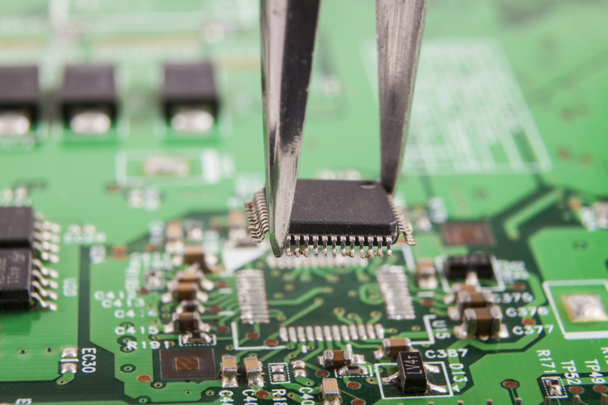
7 Critical PCB Layout Rules Every Designer Must Know in 2025?
Struggling with circuit board failures? In high-speed PCB design today, one mistake can mean costly redesigns. Follow these rules to avoid disaster. Thermal management, plane optimization, smart routing, strategic placement, early rule-setting, rigorous DRC checks, and signal integrity preservation form the core 7 rules. Mastering these prevents overheating, EMI issues, and production delays in modern […]
How to design Multilayer PCBs?

Master multilayer PCB stackup design, select high-frequency materials like Rogers RO4000, prevent defects via copper balance, and control costs with hybrid materials. DFM rules ensure reliability.

