
What is Via in Pad Technology?
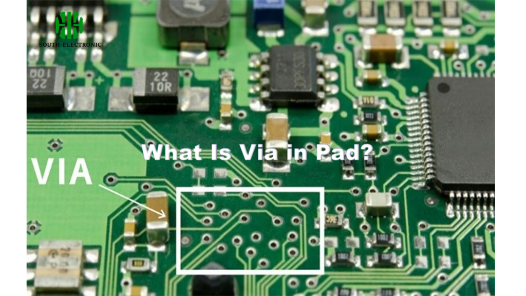
Unlock PCB potential with via-in-pad! Save space, boost signal integrity, and improve thermal management for high-density designs.
Unlock PCB potential with via-in-pad! Save space, boost signal integrity, and improve thermal management for high-density designs.
WhatsApp us
The more detailed you fill out, the faster we can move to the next step.
