

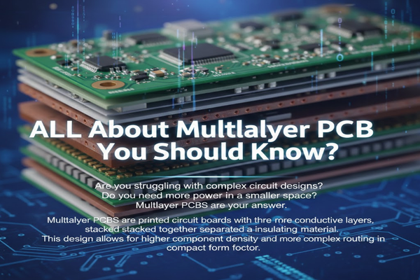
Are you struggling with complex circuit designs? Do you need more power in a smaller space? Multilayer PCBs are your answer.
Multilayer PCBs[^1] are printed circuit boards with three or more conductive layers[^2], stacked together and separated by insulating material[^3]. This design allows for higher component density[^4] and more complex routing[^5] in a compact form factor.
I remember the first time I encountered a really intricate electronic device, I wondered how they packed so much functionality into such a tiny space. It turns out, multilayer PCBs are the secret sauce behind many of our modern gadgets. Let's dig deeper into what makes them so special.
Single-Layer vs. Double-sided PCBs vs. Multilayer PCBs: What's the Difference?
Confused about PCB types? Do you wonder which one is right for your project? Understanding the differences is key.
Single-layer PCBs have one conductive layer, double-sided PCBs have two, and multilayer PCBs have three or more. This fundamental difference impacts complexity, component density, and overall functionality for electronic devices.
When I first started in electronics, the choices felt overwhelming. Single-layer boards are simple, great for basic circuits like remote controls. They are cheap and easy to make. Double-sided boards add more flexibility, letting you route traces on both sides, perfect for slightly more complex items like power supplies. But when you need to handle high speeds, dense components, or complex signals, multilayer PCBs become essential. They allow for dedicated power and ground planes, shielding, and much shorter signal paths. This makes a huge difference in performance and reliability. It's like comparing a single-lane road to a multi-lane highway—the highway handles more traffic much more efficiently.
Key Differences at a Glance
| Feature | Single-Layer PCB | Double-Sided PCB | Multilayer PCB |
|---|---|---|---|
| Layers | 1 conductive layer | 2 conductive layers | 3+ conductive layers |
| Complexity | Low | Medium | High |
| Cost | Low | Medium | High |
| Density | Low | Medium | High |
| Applications | Simple electronics, calculators | Power supplies, LED lighting | Smartphones, computers, medical devices |
| Routing | Very limited | Moderate | Highly flexible, dedicated planes |
I've personally seen projects fail because the wrong PCB type was chosen. Always match the board to your design's demands.
What is a Multilayer PCB Via?
Do you know how connections move between layers? Vias are the unsung heroes of multilayer PCBs.
A multilayer PCB via is a plated hole that electrically connects traces between different layers of a PCB. They are crucial for creating complex circuits by allowing signals to travel vertically through the board.

I remember looking at a multilayer board for the first time and wondering how the signals actually jumped from one side to the other. That's where vias come in. Think of them as tiny tunnels. They are copper-plated holes that ensure electrical conductivity between layers. There are several types, each with its own use. Through-hole vias go all the way through the board. Blind vias connect an outer layer to an inner layer but don't go through the entire board. Buried vias connect two or more inner layers and are not visible from the outside. The choice of via type depends on the density and complexity of the circuit, as well as cost considerations. Using the right via type can significantly improve signal integrity and reduce board size.
Types of Vias
| Via Type | Description | Common Use Case |
|---|---|---|
| Through-hole | Extends from the top layer to the bottom layer, visible on both sides. | General purpose, cost-effective |
| Blind Via | Connects an outer layer to one or more inner layers, but not through the entire board. | High-density interconnects, space saving |
| Buried Via | Connects two or more inner layers, completely internal to the PCB. | Very high-density designs, improved signal integrity |
Proper via design is critical; incorrect placement or sizing can lead to signal integrity issues, something I learned the hard way on an early design.
Multilayer PCB Manufacturing Process?
Ever wondered how these complex boards are made? The manufacturing process is a marvel of precision.
The multilayer PCB manufacturing process involves several key steps: inner layer fabrication, stacking and lamination, drilling and electroplating vias, outer layer patterning, solder mask and surface treatment, and final testing and quality control.
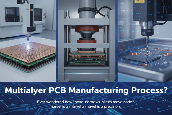
When I first visited a PCB factory, I was amazed by the sheer number of intricate steps involved. It’s not just a matter of pressing layers together; it’s a detailed, multi-stage process. First, the inner layers are prepared individually, meaning traces are etched onto the copper-clad laminate. Then comes stacking and lamination, where these pre-processed layers are carefully aligned with prepreg (a bonding material) and copper foil, then pressed together under high temperature and pressure. This creates a solid, multi-layered board. After lamination, holes are precisely drilled for vias, and these holes are then electroplated with copper to create the electrical connections. The outer layers are then patterned, solder mask is applied to protect the traces, and a surface finish is added to ensure solderability. Finally, comprehensive testing ensures every board meets specifications. This meticulous process ensures high reliability.
Key Manufacturing Steps
| Step | Description | Purpose |
|---|---|---|
| 1. Inner Layer Fabrication | Etching circuit patterns onto individual core layers. | Creates the internal conductive paths. |
| 2. Stacking and Lamination | Bonding layers with prepreg and copper foil under heat and pressure. | Forms the multi-layered structure. |
| 3. Drilling and Electroplating Vias | Creating holes and plating them with copper. | Establishes vertical electrical connections. |
| 4. Outer Layer Patterning | Etching patterns onto the top and bottom layers. | Defines external circuit paths and pads. |
| 5. Solder Mask and Surface Treatment | Applying a protective layer and a conductive finish. | Protects traces, aids soldering. |
| 6. Testing and Quality Control | Electrical and visual inspection. | Ensures functionality and adherence to standards. |
Each step demands precision; I've seen how a small error in one stage can affect the entire board's performance.
South-Electronic: A Trustful Multilayer PCB Manufacturer?
Need a reliable partner for your PCB needs? Choosing the right manufacturer is paramount for success.
South-Electronic is a trusted multilayer PCB manufacturer known for its high-quality production, advanced technology[^6], and excellent customer service[^7], making them a dependable choice for complex board requirements.

Finding a manufacturer you can trust is crucial, especially for complex multilayer PCBs. I’ve worked with various manufacturers, and what sets a good one apart is not just their technical capability but also their commitment to quality and communication. South-Electronic, for instance, has a reputation for strict quality control measures at every stage of their manufacturing process. They use state-of-the-art equipment and employ experienced engineers who understand the nuances of high-layer count boards. Their ability to handle diverse requirements, from quick-turn prototypes to large-scale production, makes them a versatile partner. They also offer strong technical support, which is invaluable when you encounter design challenges. A manufacturer's ability to consistently deliver boards that meet your precise specifications can literally make or break your project. It's about finding a partner, not just a supplier.
Why Choose a Reputable Manufacturer?
| Aspect | Benefit | Risk of Poor Choice |
|---|---|---|
| Quality Control | Reliable, functional PCBs, fewer defects. | High defect rates, project delays, rework costs. |
| Technology | Access to advanced processes for complex designs. | Limited capabilities, inability to realize advanced designs. |
| Expertise | Guidance on design for manufacturability, problem-solving. | Design flaws go unnoticed, production issues. |
| Customer Service | Clear communication, timely updates, effective issue resolution. | Misunderstandings, missed deadlines, frustration. |
| Certifications | Adherence to industry standards (e.g., ISO, UL). | Non-compliant products, safety risks. |
My experience tells me that investing in a good manufacturer saves time and money in the long run.
Conclusion
Multilayer PCBs are vital for modern electronics. Understanding their types, vias, and manufacturing ensures successful and efficient product development.
[^1]: Explore the advantages of multilayer PCBs for compact and complex circuit designs. [^2]: Learn how the number of conductive layers impacts the functionality and efficiency of PCBs. [^3]: Find out about the various insulating materials that improve PCB performance. [^4]: Understand the importance of component density in modern electronic devices. [^5]: Discover how complex routing enhances the performance of multilayer PCBs. [^6]: Discover the cutting-edge technologies that enhance PCB manufacturing processes. [^7]: Learn how effective customer service can improve your PCB manufacturing experience.

