
Can AI Truly Replace Human PCB Designer?
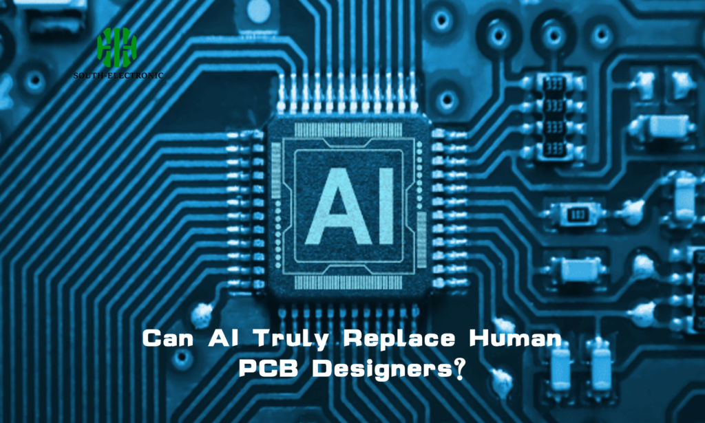
Explore whether AI can truly replace human PCB designers, analyzing strengths, limitations, and future collaboration.
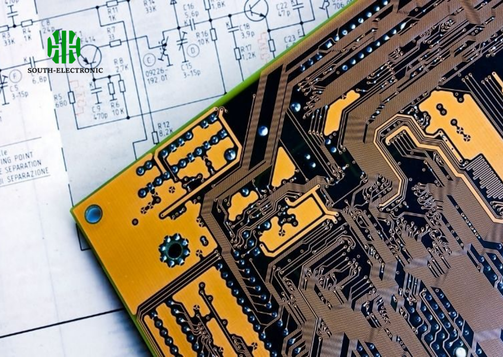
How to Deal with Crossing Wires When Designing a PCB?
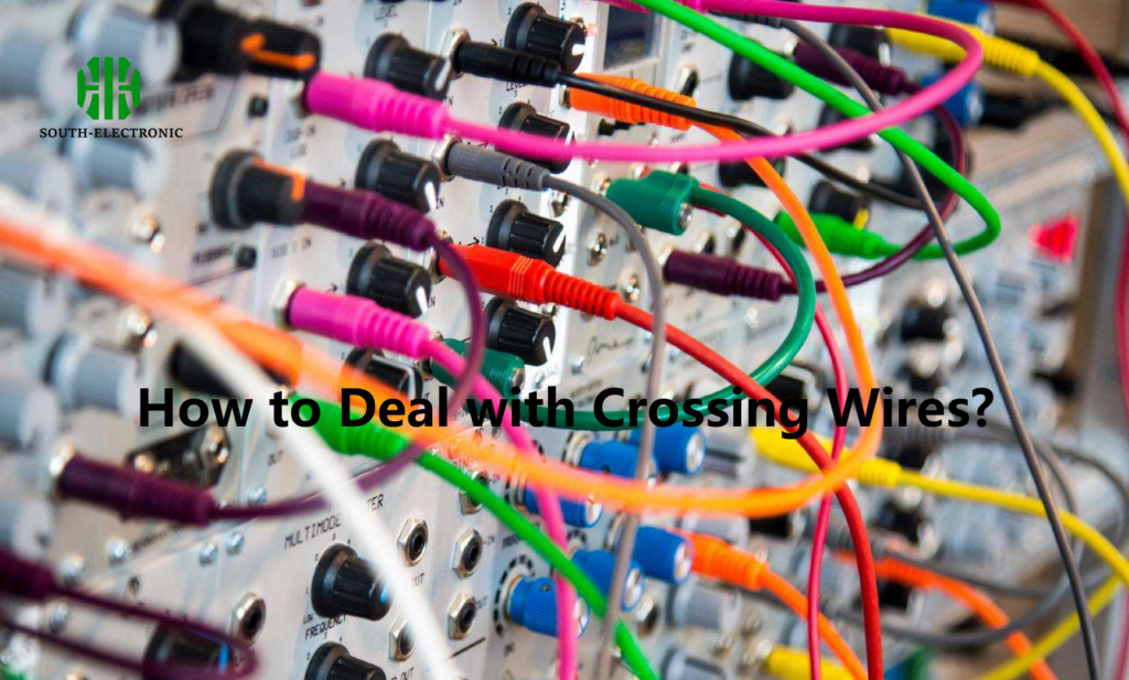
Discover how to effectively manage crossed wires in PCB design, reduce mistakes, and guarantee optimal circuit performance.
What is the Most Difficult PCB You Have Ever Designed?
Learn how to tackle the toughest PCB designs with expert advice and practical solutions.
How to Determine Impedance in a Circuit?

In this article, I’m going to show you how to accurately determine impedance in a circuit.
The 13 Most Used PCB Layout Design Tools
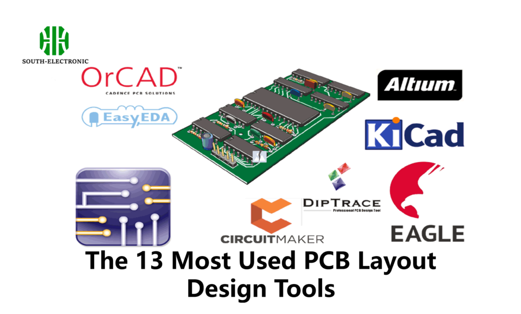
Check out the 13 most popular PCB layout design tools, from Altium Designer to CircuitMaker, and find the perfect fit for your project.
What’s the Meaning of Schematic Diagram?
Let’s delve into the details of schematic diagrams, their importance, applications, and how they differ from other diagrams like wiring diagrams.
What is a Prototype Circuit Board? Understanding Its Importance in Electronics Design
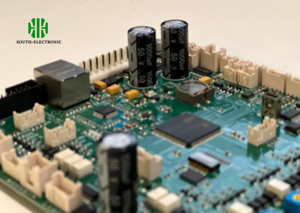
Find prototype circuit boards: The secret to testing and perfecting electronic designs before they’re mass produced.
How did you learn a PCB layout?
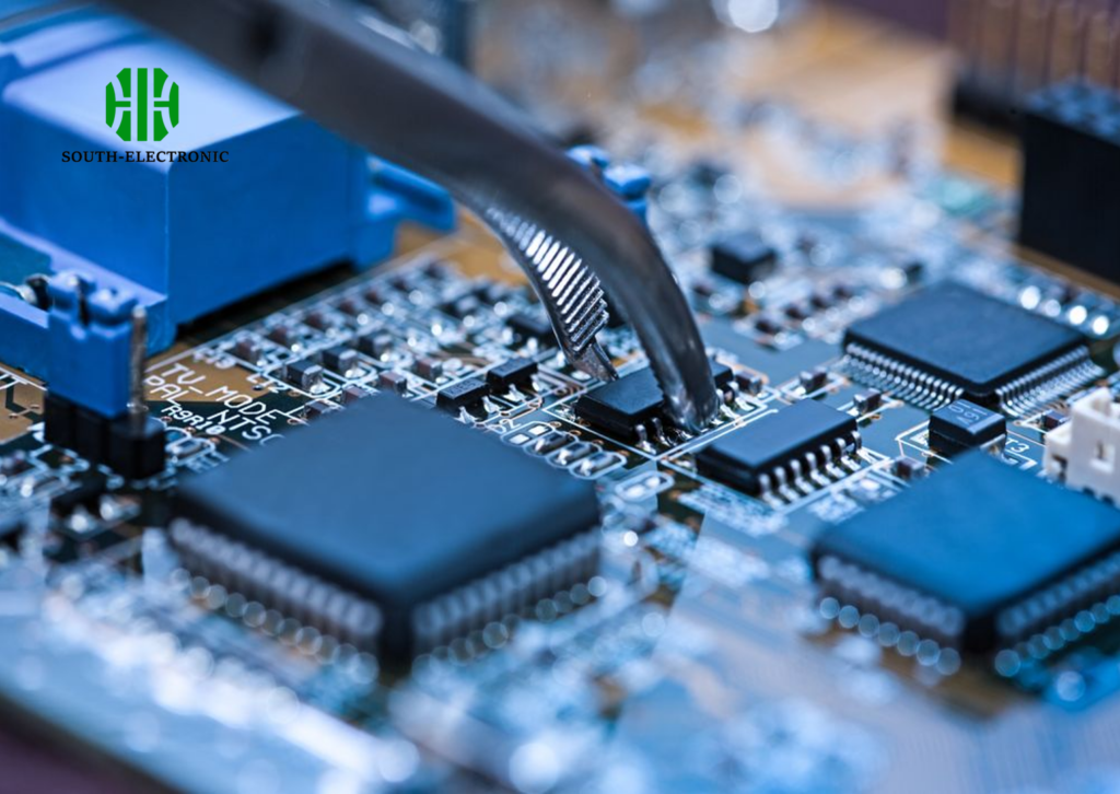
Learn how I became a PCB layout pro, conquering obstacles with real-world fixes and sharing must-know tips for newbies.
Which Layout Has More Scope: PCB or Custom IC Layout?
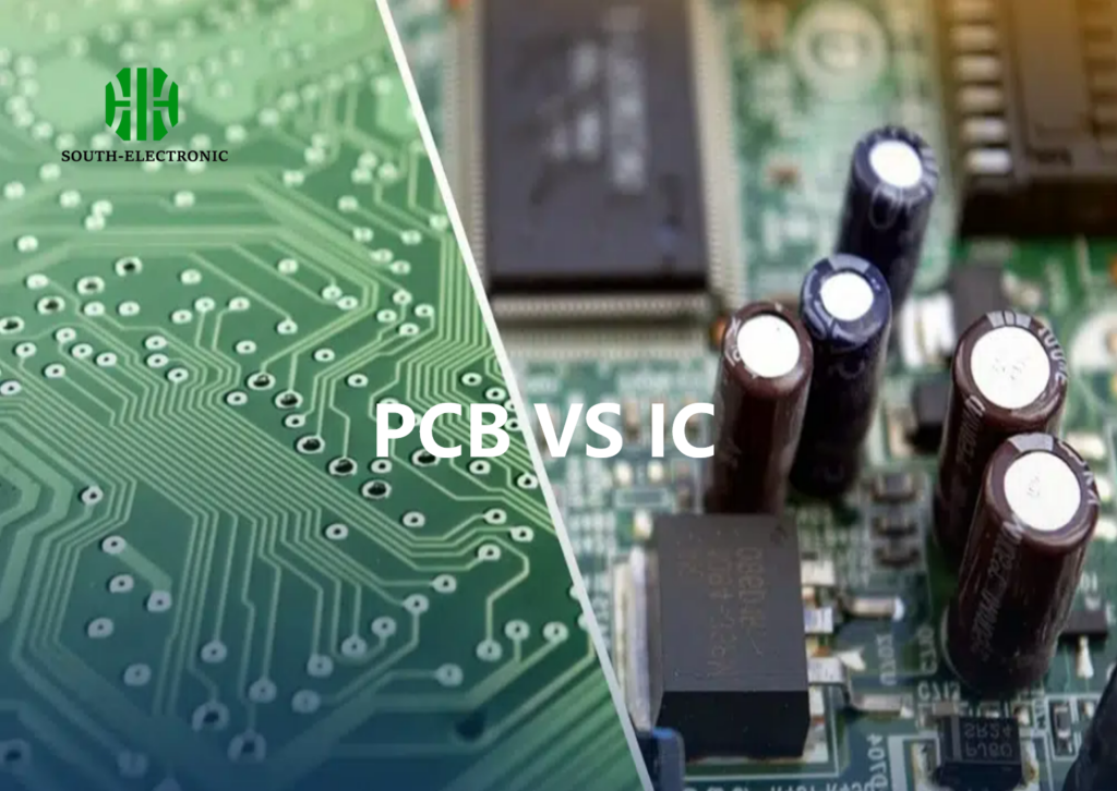
PCB layout offers broad use, while custom IC targets high-performance needs in specialized fields.
Understanding PCB Ground Planes: A Comprehensive Guide

Unlock the secrets to flawless PCB design with our in-depth guide on ground planes – essential for noise reduction and stability!
