How do you choose between shield cans and conformal coatings?
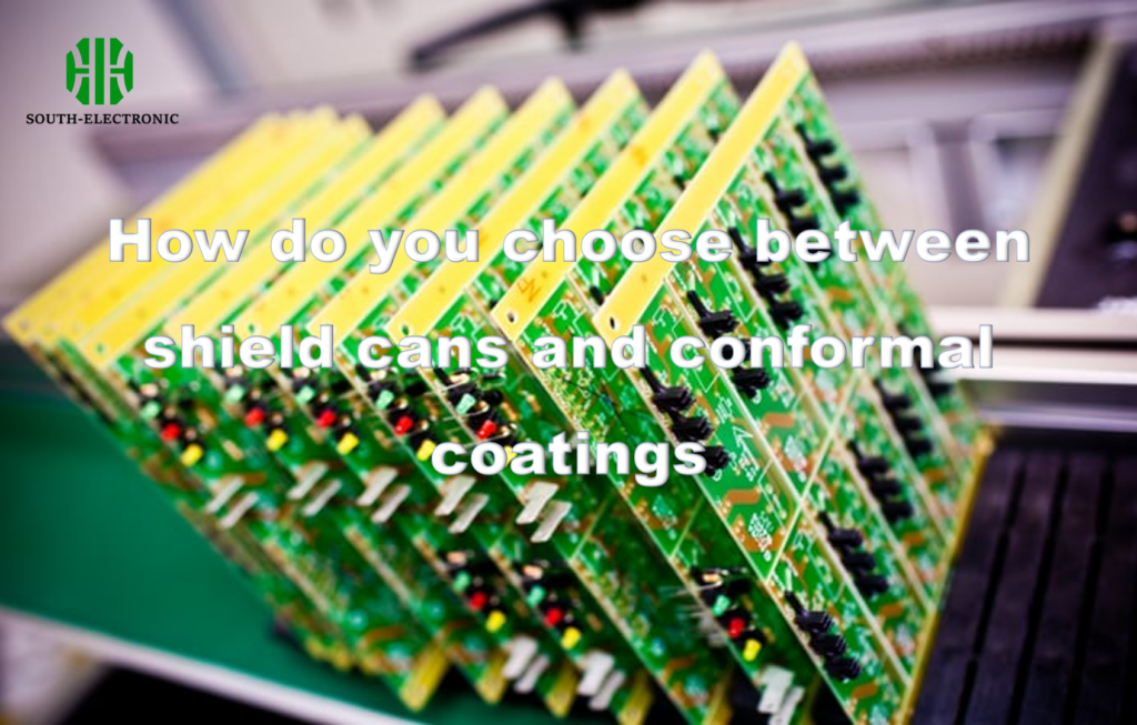
Optimize PCB shielding: Use cans for repairable EMI/impact protection and coatings for lightweight environmental sealing. Master grounding, flexible materials, and gasket cost-benefit.
What is HDI PCB and its Function?
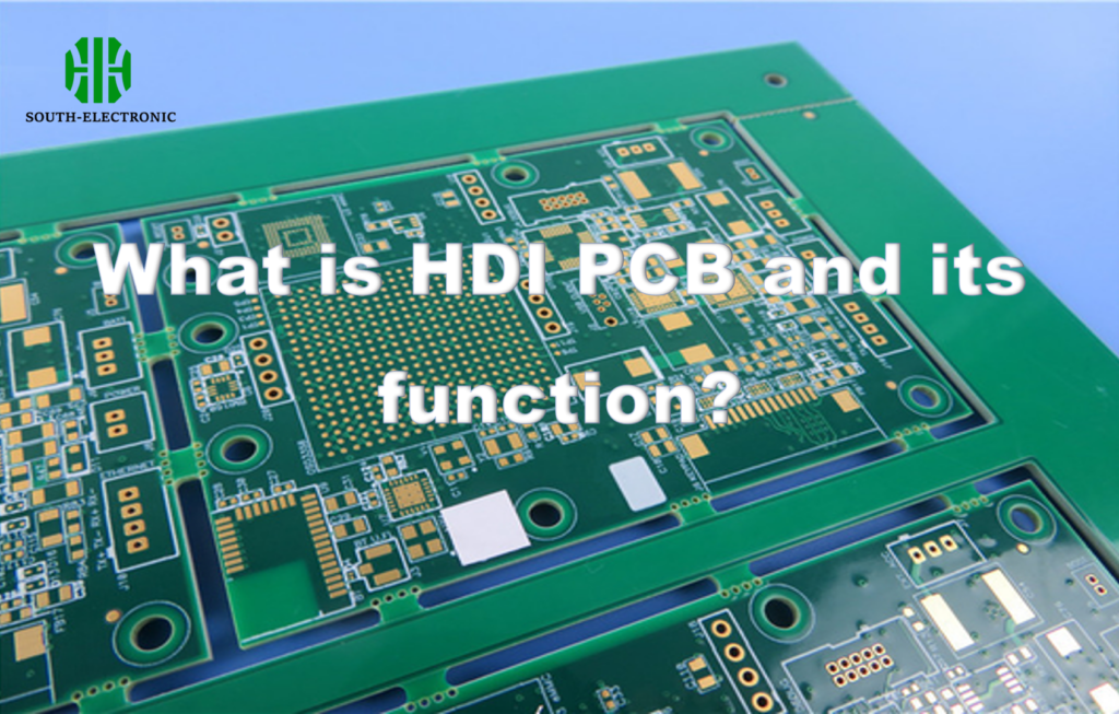
HDI PCBs use microvias for compact, high-performance electronics in smartphones, medical devices, and cars. Ultra HDI enables nano-scale circuits for aerospace/neural tech via submicro-vias and materials.
Why do microwave PCBs fail?
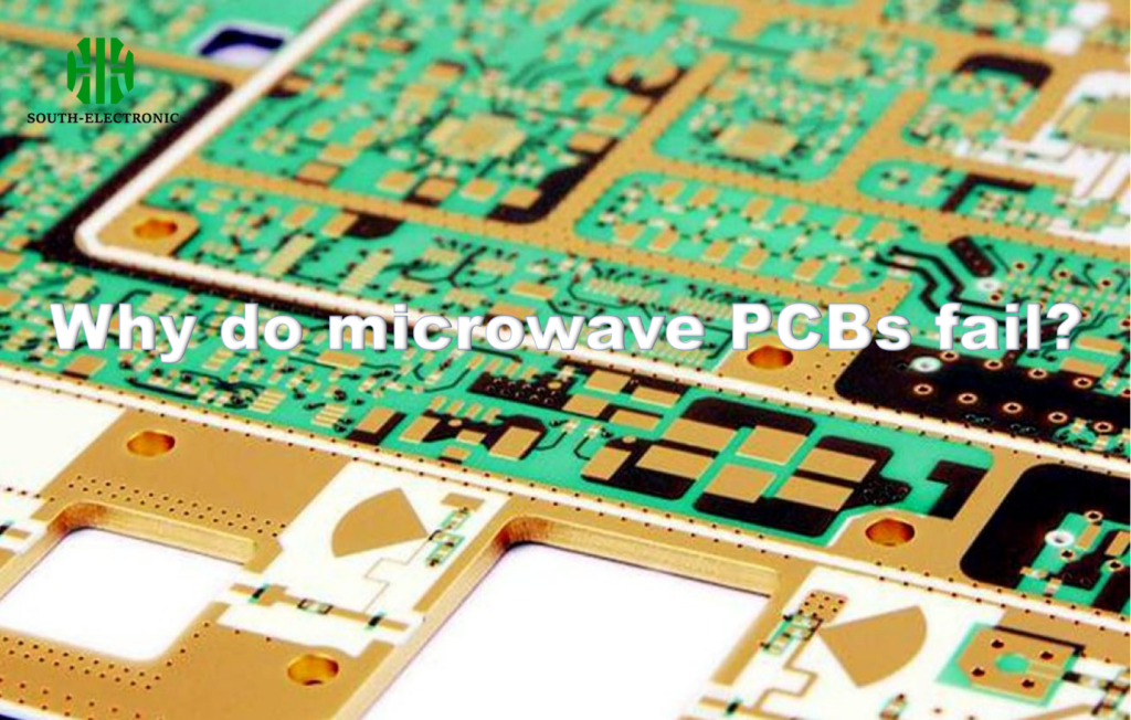
Microwave stopped working? PCB failures explained: overheating, design flaws, aging. Learn repairable vs hopeless cases & smart stackup choices to prevent future breakdowns.
SMD vs SMT: What’s the Real Difference?
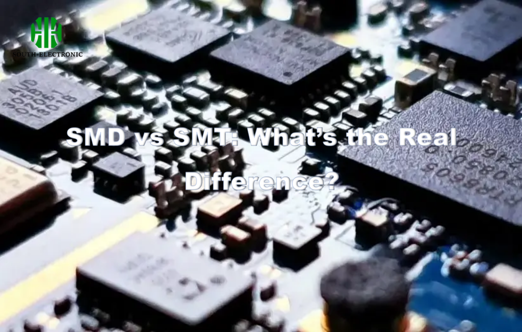
Learn the critical difference between SMD components & SMT assembly. Master SMD marking decoding, industry applications, and optimal package selection to prevent design errors.
How thick should my SMT stencils be?
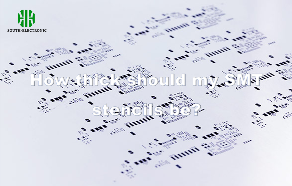
Prevent PCB overheating: choose heatsinks by material/geometry, Optimize SMT stencil thickness (0.1-0.2mm), design apertures to prevent bridges, apply coatings for fine-pitch components, and maintain stencils to extend lifespan for flawless solder paste deposition.
How Do I Pick the Right Heatsink for My PCB?
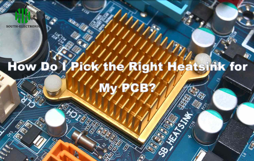
Prevent PCB overheating: choose heatsinks by material/geometry, secure with screws/clips/adhesive, add thermal vias, and avoid TIM failures or loose mounting for reliable thermal management.
What are rigid PCBs made of?
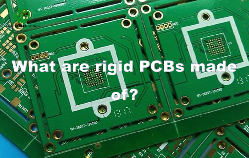
Master rigid PCB durability, cost-saving design strategies, material choices & signal integrity for high-speed applications. Choose wisely vs. rigid-flex PCBs.
What is the maximum thickness of copper in PCB?
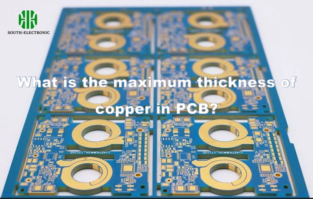
Choose PCB copper weight wisely: use 1-3oz for standard boards, 4-12oz heavy copper for high-power/heat, and 12-20oz for extreme applications. Design tips included.
What are aluminum PCBs used for?
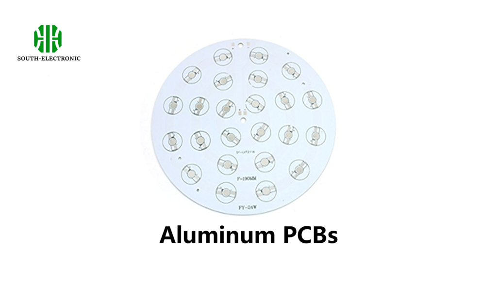
Aluminum PCBs offer 10x faster thermal conductivity than FR4. Essential for power electronics like LEDs, amplifiers & automotive apps despite higher costs. Solve overheating.
What is PCB X-ray inspection?
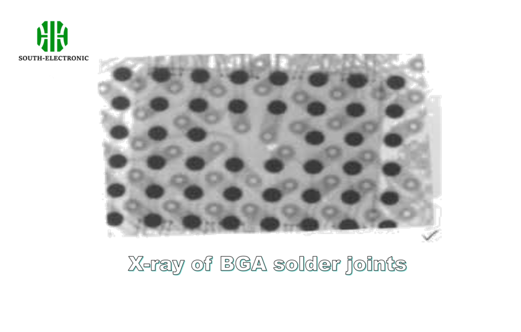
Discover how PCB X-ray inspection exposes hidden defects in BGAs/multilayer boards. Essential for medical/aerospace quality control. Learn specs & defect analysis.