
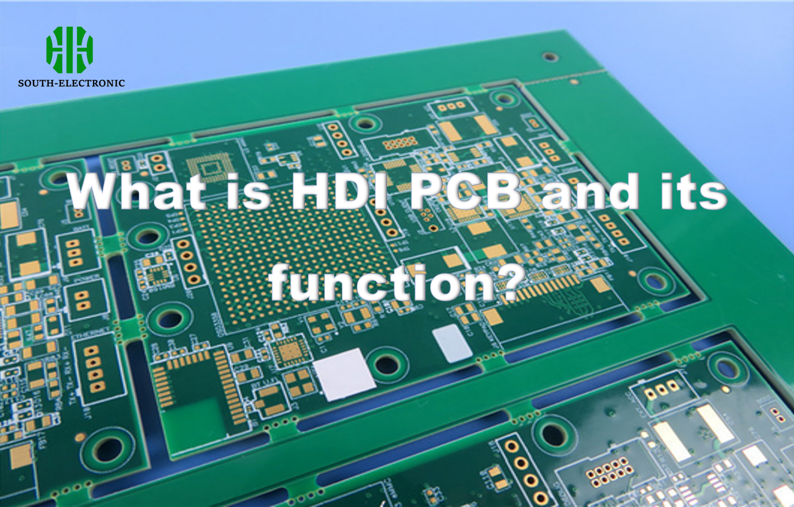
Ever tried upgrading your smartphone or wearable tech? Current devices demand minuscule circuit boards crammed with features. Standard PCBs crack under this pressure. HDI PCBs solve this miniaturization nightmare for good.
HDI (High-Density Interconnect) PCBs pack more wiring into smaller spaces using advanced techniques like microvias, significantly shrinking electronics while boosting performance for smartphones, medical gear, and vehicles.
But knowing what HDI is isn’t enough—you must grasp how it beats alternatives. I’ll break down key comparisons and next-gen applications in plain terms below.
What is the difference between HDI PCB and normal PCB?
Watch bulky gadgets struggle with slow signal speeds? Standard PCBs cause these limitations. HDI tackles this using smarter via designs.
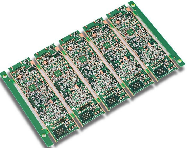
Normal PCBs use larger through-hole vias spanning all layers wasting space. HDI employs microvias less than 0.15mm wide, enabling 3x denser routing for slimmer gadgets like smartwatches.
Why via design changes everything
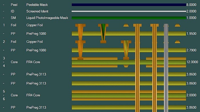
Normal PCBs rely on Plated Through Holes (PTH) passing through every layer. This restricts component placement and increases size substantially. In contrast, HDI boards use three space-saving techniques:
| Feature | Normal PCB | HDI PCB |
|---|---|---|
| Via Type | Full PTH only | Microvias/Buried/Blind |
| Line Width | 150-300μm | Under 100μm |
| Layers Impact | All layers cut | Selective layers |
| Use Case | Simple LEDs | Smartphones |
Blind vias connect outer layers to inner ones without penetrating fully. Buried vias link inner layers invisibly. Stacking these allows vertical "subway systems" for signals. This trims board size by 70% compared to traditional layouts. Faster signal paths also cut lag in 5G devices.
What is the difference between PTH and HDI PCB?
See heat issues or cracks in industrial controllers? Plated Through Hole (PTH) technology often struggles under stress. HDI avoids these failures with precision.
PTH creates holes drilled through all layers and plated with metal. These holes waste space and weaken structures. HDI uses laser-drilled microvias targeting specific layers, preserving strength while saving space for delicate implants.
Beyond basic connections
PTH and HDI serve different complexity levels:
| Factor | PTH | HDI |
|---|---|---|
| Size | 300+ microns | 50-100 microns |
| Heat Resistance | Low (delamination risk) | High (refined materials) |
| Layer Flexibility | Fixed routing | Dynamic stacking |
| Cost Efficiency | Cheap for simple boards | Saves long-term via miniaturization |
PTH vias behave like highways crossing every neighborhood—slow and invasive. HDI’s buried/blind vias act as express tunnels between districts. For pacemakers, this means fewer layers but smarter connections avoiding signal interference. Sequential lamination in HDI also prevents warping in car sensors.
What is ultra HDI PCB?
Need extreme precision for aerospace or neural sensors? Standard HDI hits limits around 40μm circuits. Ultra HDI pushes boundaries below 20μm.
Ultra HDI employs submicro-vias under 50μm and specialized materials enabling record density. This allows pixel-perfect circuits for VR headsets and satellite trackers where millidegree accuracy matters.
Cutting-edge vs. conventional HDI
| Parameter | HDI PCB | Ultra HDI |
|---|---|---|
| Line/Space | 60μm/60μm | 25μm/25μm |
| Via Diameter | 100μm microvias | 25μ submicro vias |
| Layer Count | Up to 16 layers | 30+ layers |
| Materials | FR-4 base | Low-CTE polyimide |
| Failures/Million | 5000 defects | Under 200 defects |
Laser direct imaging replaces photomasks for flawless 6μm traces. Semi-additive processes build circuits chemically rather than etching. This eliminates undercuts threatening microchips in rockets. Crucially, low-thermal-expansion laminates prevent cracks during orbital temperature swings.
Conclusion
HDI PCBs revolutionized miniaturization using microvias. Ultra HDI now pioneers nano-scale designs, making impossibly smart devices accessible to everyone. Upgrade your prototypes wisely.

