
The construction of component packaging is an important part of PCB design. A small mistake may cause the entire board to not work and cause serious delays in the construction period. Therefore, it is important for every PCB engineer to have relevant knowledge of component packaging.
PCB packaging is to express various parameters of actual electronic components, chips, etc. (such as component size, length and width, direct plug, patch, pad size, pin length and width, pin spacing, etc.) in a graphical way so that it can be called when drawing PCB diagrams.
What are the types of component packaging?
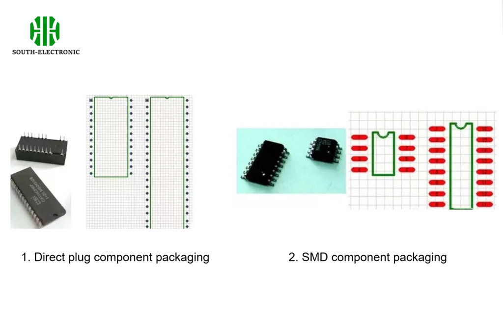
The packaging is mainly divided into two types: DIP dual in-line plug and SMD patch packaging.
-
Direct plug component packaging
The pads of direct plug component packaging generally run through the entire circuit board, from the top layer to the bottom layer, and the pins of the components are soldered, as shown in the figure.
Image -
SMD component packaging
SMD components refer to components whose pads are only attached to the top or bottom layer of the circuit board, and the welding of components is carried out on the working layer of the assembled components.
What are the common component packages?
For most electronic components, common discrete component packages mainly include diodes, capacitors, resistors and transistors; common integrated circuits mainly include single-in-line and dual-in-line.
- Diodes: The number of diode component packages is generally DIODE-xx, where the number xx represents the distance between the pins of diode components. For example, the component package number DIODE-0.5 means that the distance between the component pins is 500mil.
- Capacitors: Capacitor component packages can be divided into two categories, namely non-polar capacitors and polar capacitors. The number of non-polar capacitor component package is RADxx, where the number xx indicates the distance between the component package pins; the number of polar capacitor component package is RBxx-yy, where the number xx indicates the distance between the component pins, and the number yy indicates the diameter of the component.
- Resistor: Resistor component packages can also be divided into two categories, namely ordinary resistors and variable resistors. The number of ordinary resistor component packages is AXIAL-xx, where the number xx indicates the distance between the component pins; the number of variable resistor component packages is VRx, where the number x indicates the category of the component.
- Integrated circuit category: The number of single-row in-line component packages is SIL-xx, where the number xx indicates the number of pins of the single-row in-line integrated circuit; the number of dual-row in-line component packages is DIP-xx, where the number xx indicates the number of pins of the dual-row in-line integrated circuit.
Constituent elements of component package
To form a component package, three main elements should be paid attention to:
-
Pads – used to fix the device to the circuit board and connect signals with other devices through wires. We need to draw the shape, position and pad number of the device according to the data sheet. The number corresponds to the pin number of the device;
-
Outline – The outline of the component package is to tell the designer the area occupied by the device. No other device can be placed within the outline, otherwise it will cause a conflict;
-
Silkscreen marking – We need to mark the key information of the device through silkscreen, such as which pin is the starting pin? The polarity and direction of the device, etc.
In addition to the above three major elements, most CAD software has added 3D data. Based on these data, designers can know the three-dimensional shape of the device, which is very important in mechatronics design.
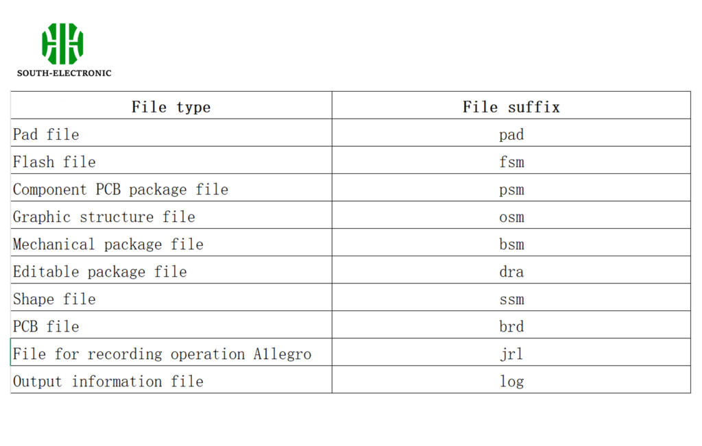
The meaning of the package file suffix
In Allegro software, the meaning of the file suffixes of some common PCB packages are as follows:
Conclusion
PCB component packaging is crucial for design, covering types, common packages, elements, and suffix meanings to ensure board functionality.

