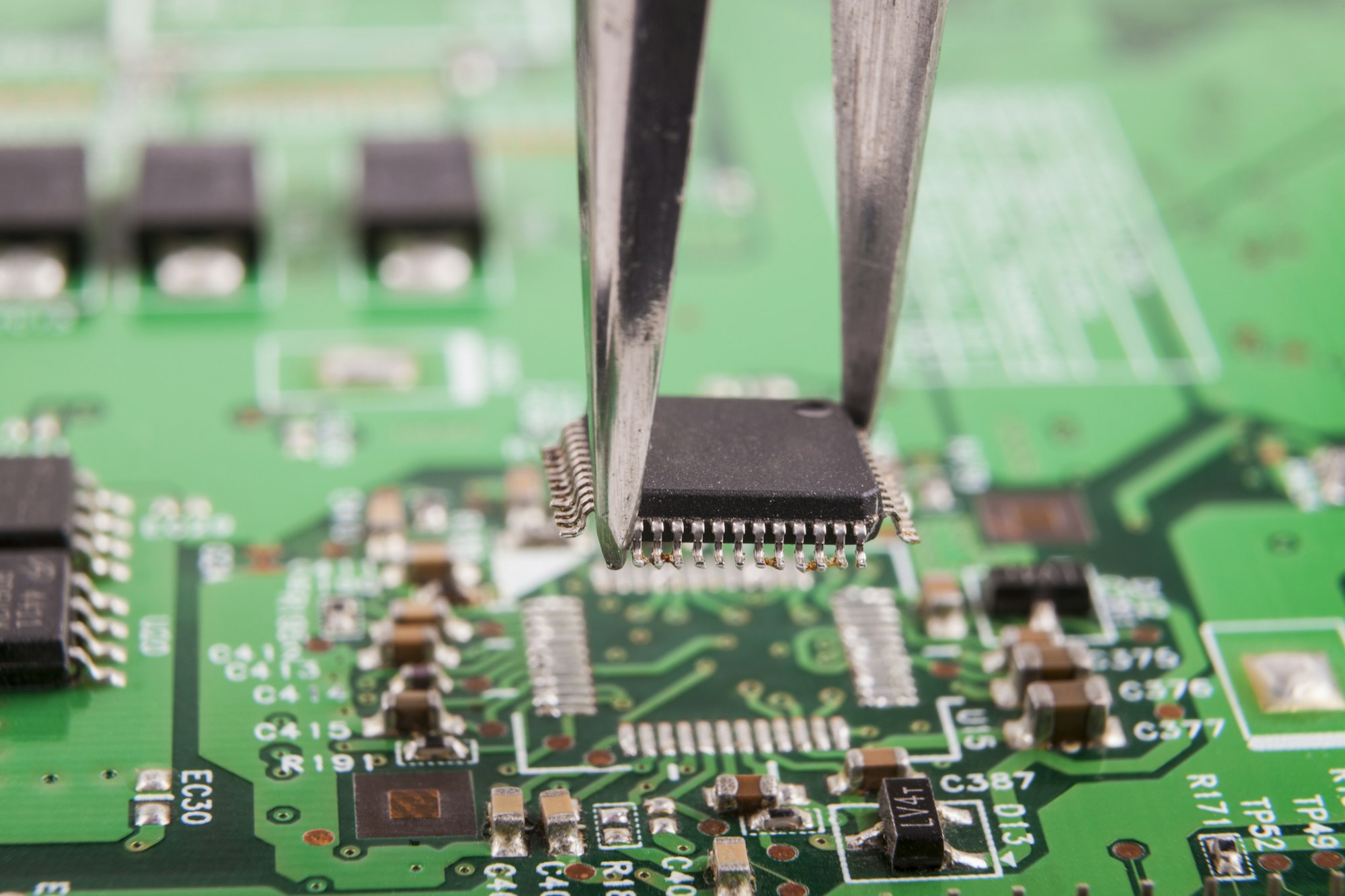
I had a project halted by a wrong board choice. I panicked, then I learned the key PCB categories. I now pick the right board fast.
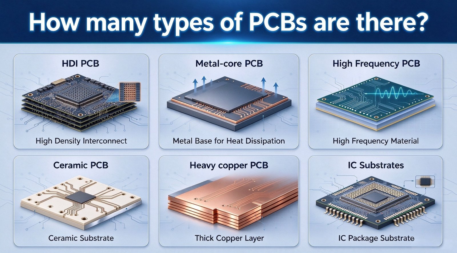
PCBs are most commonly classified by layer count: single-sided PCBs, double-sided PCBs and multilayer PCBs.They can also be grouped according to mechanical properties: rigid PCBs (e.g. FR-4), flexible PCBs (FPC), and rigid-flex PCBs. Another classification is based on special technologies and materials: HDI PCBs, metal-core PCBs (MCPCB / aluminum PCBs), high-frequency PCBs (using Rogers, PTFE and other materials), ceramic PCBs, heavy copper PCBs, and IC substrates. Today we will focus on the third category — PCBs defined by special technologies and materials. This helps you pick the right board fast.
I will walk through each main type one by one. I will share when I use each board. I will keep examples clear. I want you to choose the right PCB with less risk.
HDI PCBs – High Density Interconnect PCBs
I once tried to route a complex phone board the old way. I failed and then met HDI. I saved space and improved speed.
HDI PCBs use microvias, blind and buried vias, and fine traces to increase wiring density and improve signal paths. They shrink size and help high I/O designs.
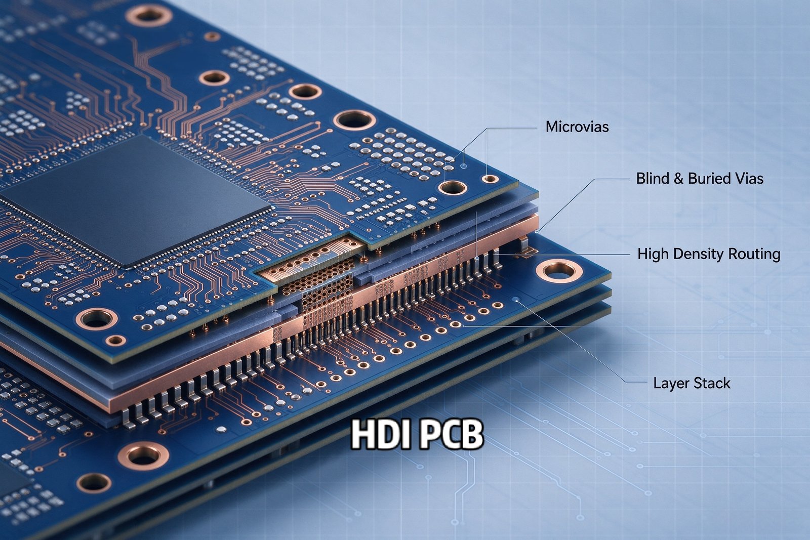
I explain why HDI matters and how I design it. I start with microvias. I place them to shorten traces and avoid long jumps. I add stacked or staggered vias when I need more layers. I pick high-quality FR-4 or specialized laminates based on frequency and thermal needs. I check types of pcb materials to match dielectric constant and Tg. I consult a types of pcb materials pdf when I need precise numbers. I set tight trace and spacing rules early. I keep solder mask and surface finish in mind for assembly. I work with the board house to confirm process limits. Below is a simple view of via types and when I use them.
| Via type | When I use it |
|---|---|
| Microvia | For layer-to-layer short jumps |
| Blind via | To connect outer to inner layers only |
| Buried via | To hide connections inside layers |
| Stacked via | When I need dense vertical routing |
I test prototypes for impedance and routing yield. I change the stack-up when I see signal issues. I pick HDI when size and performance beat cost.
Metal-core PCB
If you’ve dealt with LEDs and power components getting scorching hot during operation, you know the frustration all too well. That trapped heat eats away at your parts, cutting their service life short and bringing unexpected, frequent failures that derail your project. The good news? Metal-core PCBs quickly draw heat away from heat-generating LEDs and power circuits, easing thermal stress and helping your hardware run reliably for longer.
MCPCBs use a metal base, often aluminum, bonded to a copper circuit by a dielectric layer to improve thermal transfer. They cut junction temperatures and boost reliability in power parts.
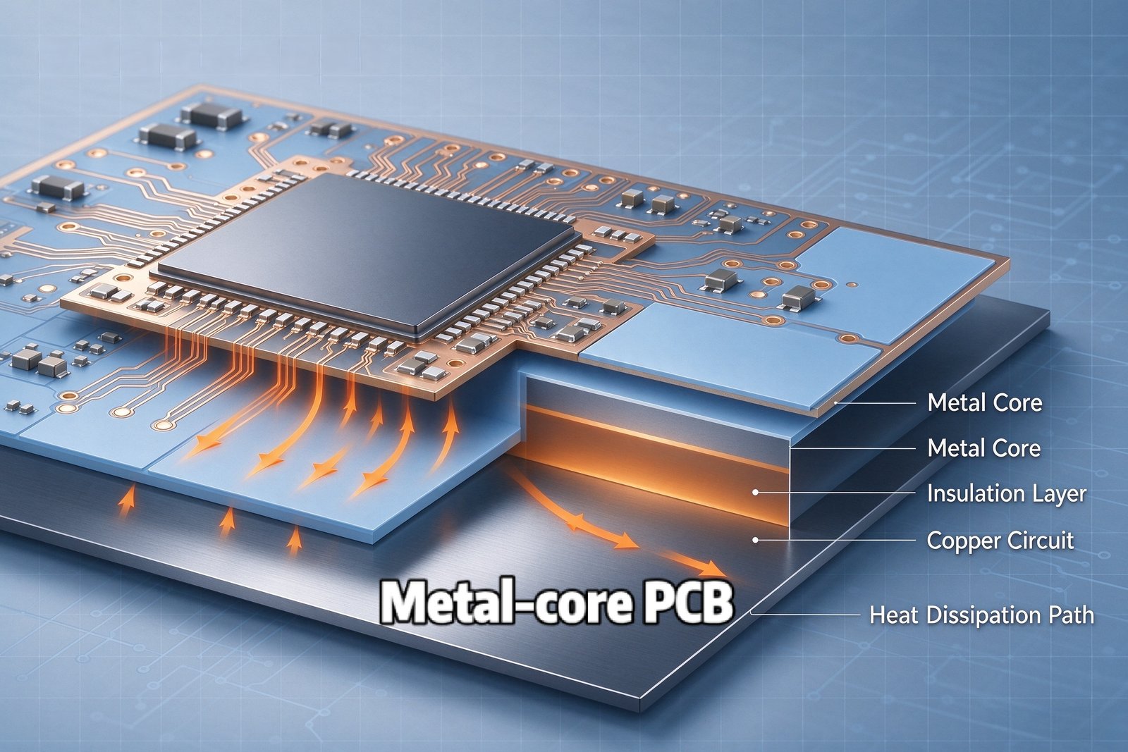
I break down MCPCB layers and when I choose them. The base is metal, usually aluminum or copper. A dielectric layer sits on the metal. Copper foil is on top for the circuit. I place devices so heat flows from the device to the metal. I pick aluminum when I need light weight and good cost. I pick copper when I need extreme thermal conductivity. I use MCPCB for LEDs, power modules, and motor drivers. I watch for soldering limits and finish choices. I often check pcb used for thermal management before finalizing. Below is a quick comparison.
| Layer | Role |
|---|---|
| Metal base | Heat spreader and structure |
| Dielectric | Bond and thermal bridge |
| Copper traces | Circuit and pads |
I must design the thermal path early. I add thermal vias when the design needs it. I confirm assembly rules with the vendor. I pick MCPCB when thermal control beats extra cost.
High Frequency PCB
I had a radio prototype that lost signal due to wrong board material. I switched to a high-frequency PCB. I then improved the signal margin.
High-frequency PCBs use low-loss laminates like Rogers or PTFE to keep dielectric loss low and impedance stable for RF and microwave signals. They suit antennas, filters, and RF front-ends.
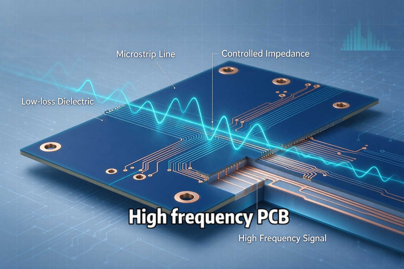
I list materials and layout rules for high-frequency designs. I pick Rogers, PTFE, or special ceramics based on loss tangent and dielectric constant[^1]. I set stack-up to control impedance. I use microstrip or stripline traces and avoid vias in critical paths. I minimize discontinuities and keep trace bends smooth. I test for insertion loss at the target band. I review the types of pcb materials pdf to compare loss tangent and thickness. I check thermal and mechanical properties[^2] because RF parts can heat up. I also note assembly constraints, since some laminates need special handling. The table below shows common laminate trade-offs.
| Material | Strength | Typical use |
|---|---|---|
| FR-4 | Cheap, higher loss | Low GHz |
| Rogers | Low loss, stable | Microwave |
| PTFE | Very low loss, hard to process | High GHz |
I prototype early and measure S-parameters. I tune the layout and then lock the design. I choose high-frequency PCBs when signal loss matters most.
Ceramic PCB
I had a module that needed high temperature and low loss. I tried ceramic PCB and then the module ran cooler and more stable.
Ceramic PCBs use alumina, aluminum nitride, or silicon nitride for stable dielectric properties and high thermal conductivity. They work well in high-power RF and harsh environments.
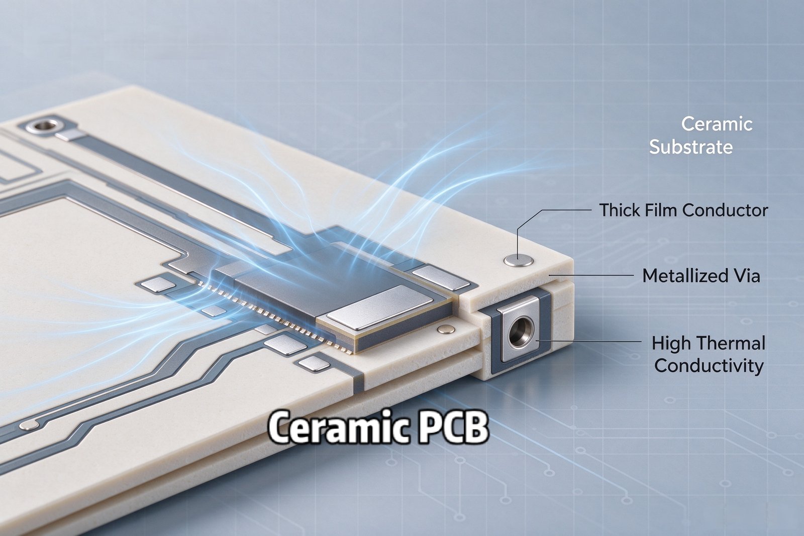
I show why ceramics suit certain jobs and where I use them. Alumina gives good dielectric stability at a lower cost. Aluminum nitride gives better thermal conduction and suits hot parts. Silicon nitride can be used for special strength needs. I use ceramic PCBs in high-power RF, space, and high-temperature sensors. I prepare the design for brittle handling and strict assembly steps. I check pcb in medical use when I need biocompatible and stable materials for implants or diagnostic gear. I compare key properties in this table.
| Ceramic | Thermal | Dielectric |
|---|---|---|
| Alumina | Good | Stable |
| AlN | Very good | Stable |
| Si3N4 | Good | Stable |
I talk early to ceramic fabricators about vias and metalization. I test for thermal cycling and mechanical shock. I use ceramic PCBs when stability and heat removal outweigh cost and handling limits.
Heavy copper PCB
I worked on a motor controller that needed thick traces. I used heavy-copper PCB and the traces did not overheat.
Heavy copper PCBs have thicker copper layers, often 3 oz or more, to handle high currents and improve thermal paths. They suit power electronics, bus bars, and welding control.
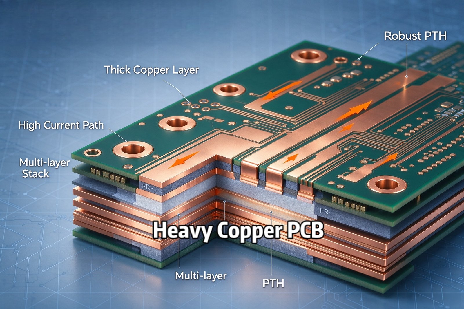
I explain copper weights and why I pick them. Standard copper is 1 oz (35 µm). Heavy copper starts at 3 oz and can go much higher. I design wider traces and add thermal vias for heat spread. I plan for heavier through-hole plating for mechanical strength. I check manufacturer limits for etch compensation and plating thickness. I use heavy copper for power converters, battery management, and motor controllers. I include a simple copper weight guide.
| Copper weight | Typical use |
|---|---|
| 1 oz | General PCB |
| 3 oz | Moderate power |
| 6+ oz | Heavy current, bus bars |
I confirm bend and finish choices. I test for current capacity and temperature rise. I pick heavy copper when pcb used for high current and heavy duty applications.
IC Substrates for Advanced Packaging & Flip Chip
I once packaged a high-speed ASIC. I used IC substrates and I achieved fine interconnect and short paths.
IC substrates are high-density bases that connect a die to the PCB. They provide short interconnects, high I/O support, and fine geometry for flip-chip and advanced packages.
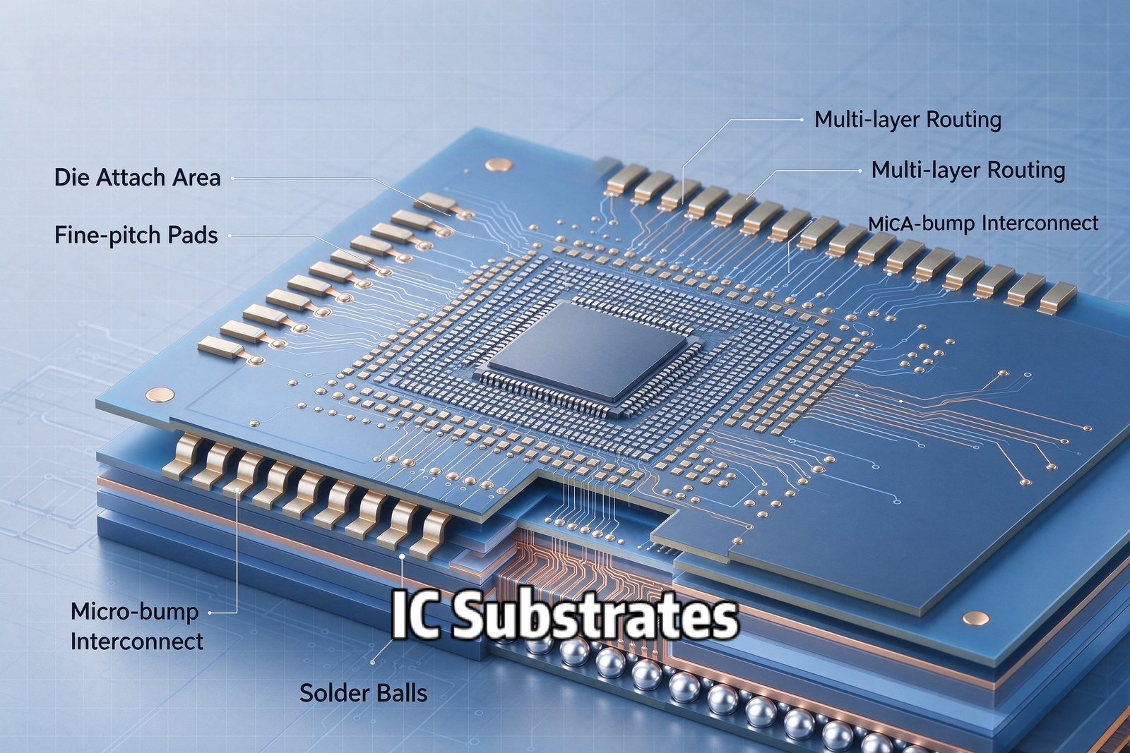
I outline substrate structure and when I use it. Substrates use fine traces, microvias, and thin build-ups. They often use BT resin, polyimide, or ceramic cores. I use them for high-performance CPUs, GPUs, and mobile processors. I design the substrate for short signal paths and tight impedance control. I compare substrate roles to PCB roles to show the difference in density and purpose. I also explain pcb board meaning and pcb full form in electrical to non-engineers: PCB stands for Printed Circuit Board and it serves as the main wiring base. IC substrates bridge the die to that main board. I often share a types of pcb materials pdf with the packaging team so we match materials and reliability tests.
| Aspect | PCB | IC Substrate |
|---|---|---|
| Density | Lower | Much higher |
| Role | Board-level wiring | Package-level wiring |
| Use | Modules and systems | Die interconnect and package |
I plan testing and thermal paths early. I work with the package vendor to align design rules. I pick substrates when chip speed and I/O count demand it.
Conclusion
I summarized the main PCB families and when I choose each type to help you pick the right board. Now you know these specialty PCB options. Turn to South-Electronic for reliable custom fabrication. Send your specs to inquiry@southelectronicpcb.com, and let’s get your project on track.
[^1]: "Dielectric loss", https://en.wikipedia.org/wiki/Dielectric_loss. [^2]: "Ultimate PCB Material Selection and Properties Guide", https://www.mclpcb.com/blog/pcb-material-selection-guide/.
<!--[googlesitekit-end-of-content]-->