
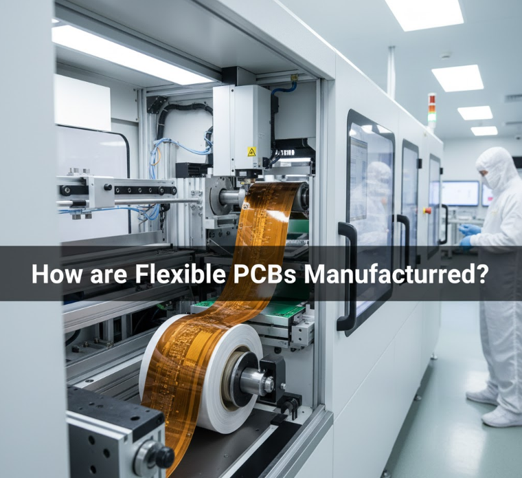
Are you curious about the tiny, bendy circuits inside your gadgets? These flexible PCBs are everywhere, making modern tech possible. How do they come to life?
Flexible PCBs are made through a precise process involving flexible polymer films, conductive materials, and photolithography. This allows circuits to be thin, bendable, and adapted to complex shapes without breaking, unlike rigid boards.
It's fascinating to peel back the layers and see how these essential components are brought into existence. Let's dive into the world of flexible PCB manufacturing and understand each step.
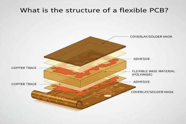
What is the structure of a flexible PCB?
Ever wondered what makes flexible circuits so adaptable? The secret lies in their unique layered construction, which is quite different from traditional rigid boards.
A flexible PCB is built on a flexible polymer film, such as polyimide, acting as the base. Conductive traces, usually copper, are then patterned onto this film, creating the electrical pathways needed for components.
When I first learned about flexible PCBs, I was amazed at how different they are from the rigid boards I was used to seeing. Their structure is the key to their flexibility and strength.
Base Material: The Flexible Foundation
The core of any flexible PCB is its base material. This is typically a thin, insulating polymer film. Polyimide (PI) is a common choice because it offers excellent thermal stability, chemical resistance, and, most importantly, flexibility. Other materials like PET (polyester) or PEN (polyethylene naphthalate) are also used depending on the application’s needs. This film provides the mechanical support and electrical insulation for the circuit.
Conductive Layer: The Electrical Pathways
On top of the base material, we find the conductive layer. This is usually made of copper. The copper is deposited or laminated onto the flexible film. The thickness of this layer can vary, ranging from very thin foils for highly flexible applications to thicker layers for higher current carrying capacities.
Adhesive Layer: Bonding It All Together
Sometimes, an adhesive layer is used to bond the copper to the base film. These adhesives must also be flexible and able to withstand the manufacturing processes. Acrylic adhesives are frequently employed for this purpose due to their good adhesion and flexibility.
Coverlay/Soldermask: The Protective Shield
To protect the delicate copper traces from environmental damage, short circuits, and contamination, a coverlay or soldermask is applied. A coverlay is a flexible insulating film, often made of polyimide with an adhesive, that is laminated over the circuit. Soldermask, similar to that used on rigid PCBs, can also be applied as a liquid or film. This layer ensures the circuit's reliability and longevity.
Surface Finish: Ensuring Solderability
Finally, the exposed copper pads, where components will be soldered, receive a surface finish. This finish protects the copper from oxidation and ensures good solderability. Common surface finishes include Electroless Nickel Immersion Gold (ENIG), Organic Solderability Preservatives (OSP), or Immersion Tin.
This multi-layered approach gives flexible PCBs their unique combination of electrical performance and mechanical flexibility.
| Layer Type | Material Example | Function |
|---|---|---|
| Base Material | Polyimide (PI) | Provides flexibility and insulation |
| Conductive Layer | Copper | Forms electrical pathways |
| Adhesive | Acrylic | Bonds copper to base (if needed) |
| Coverlay/Mask | Polyimide | Protects traces from environment |
| Surface Finish | ENIG, OSP, Immersion Tin | Ensures solderability of exposed pads |
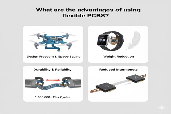
What are the advantages of using flexible PCBs?
Why do engineers choose flexible PCBs over rigid ones? The benefits extend far beyond just being able to bend them, offering significant design and performance advantages.
Flexible PCBs offer unmatched design freedom, allowing circuits to fit into tight or irregular spaces. They save space and weight, reduce interconnects, and provide excellent durability, making them ideal for compact and high-performance electronics.
I remember working on a project where space was incredibly tight. A rigid PCB simply wouldn't fit. That's when flexible PCBs became a game-changer, and I truly understood their value.
Space and Weight Savings
Flexible PCBs are inherently thin and light. This reduces the overall size and weight of electronic assemblies, which is crucial for portable devices, wearables, and aerospace applications. By conforming to tight spaces, they eliminate the need for bulky connectors and wiring harnesses, further contributing to a compact design. This small footprint is a major design advantage.
Design Freedom and Form Factor
The ability to bend, fold, and twist allows designers to create products with innovative shapes and configurations. This means electronics can be integrated into curved surfaces or very small enclosures, opening up new possibilities for product design that rigid boards simply cannot achieve. My own experience showed me how much more creative we could be with flexible boards.
Reduced Interconnects and Improved Reliability
Flexible PCBs can often integrate multiple rigid boards and their connecting wires into a single, seamless circuit. This drastically reduces the number of solder joints and connectors, which are common points of failure. Fewer connections mean higher reliability and fewer potential manufacturing defects. It's a simpler, more robust solution.
Durability Under Vibration and Motion
Unlike rigid boards, flexible PCBs can withstand repeated flexing, vibrations, and mechanical shocks without damage. This makes them ideal for dynamic applications where components are subject to movement, such as in robotics, medical devices, and automotive systems. Their resilience prolongs product life.
Enhanced Electrical Performance
Due to their thinner dielectric materials and controlled impedance characteristics, flexible PCBs can offer better signal integrity and higher-speed data transmission. They can also manage heat dissipation more effectively in certain configurations, contributing to overall system performance.
| Advantage | Description | Key Benefit |
|---|---|---|
| Space & Weight | Thin and light, fits tight enclosures | Compact and portable designs |
| Design Freedom | Bends, folds, twists to fit any any shape | Innovative product form factors |
| Reduced Interconnects | Integrates multiple parts into one circuit | Higher reliability, fewer failure points |
| Durability | Resists vibration, shock, and repeated flexing | Longer product life in dynamic applications |
| Electrical Performance | Better signal integrity, controlled impedance | Faster data, improved system performance |
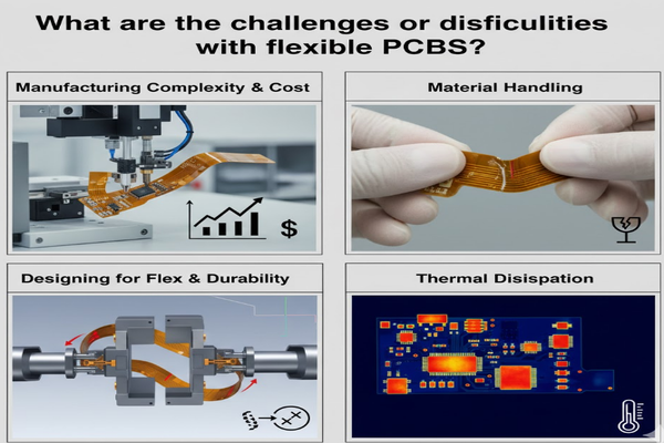
What are the challenges or difficulties with flexible PCBs?
While flexible PCBs offer many benefits, they also come with their own set of challenges. What are the hurdles engineers face when working with these versatile circuits?
Flexible PCBs present manufacturing complexities, higher material costs, and specific handling requirements due to their delicate nature. Designing for repeated flexing and managing thermal dissipation also require careful consideration, adding to their difficulty.
I learned firsthand that "flexible" doesn't always mean "easy." When I started using flexible PCBs, I encountered some unexpected difficulties that required new approaches.
Higher Manufacturing Costs
The materials used for flexible PCBs, such as polyimide films and specialized adhesives, are generally more expensive than those for rigid PCBs. The manufacturing processes also involve more intricate steps, tighter tolerances, and specialized equipment, leading to higher production costs per unit. This can be a significant barrier for budget-sensitive projects.
Design Complexity
Designing for flexibility requires a different mindset. Engineers must consider bend radii, stress points, and the effects of repeated flexing on traces and components. Managing impedance and crosstalk in dynamic environments can also be more complex. Poor design can lead to early failure.
Assembly and Handling Difficulties
Flexible PCBs are delicate and can be easily damaged during assembly if not handled carefully. They are prone to tearing, creasing, or stretching if improper tools or techniques are used. Attaching components and connectors to a flexible substrate requires precision and specialized soldering processes, making automation sometimes more challenging.
Thermal Management
While flexible materials can handle high temperatures, dissipating heat from components mounted on a flexible substrate can be tricky. The thin nature of the material may not always provide sufficient thermal pathways, requiring creative solutions like thermal vias or heat spreaders. This becomes a concern, especially with high-power components.
Repair Limitations
Repairing a damaged flexible PCB can be very difficult, sometimes impossible. The fine traces and delicate base material make rework challenging. Often, a damaged flexible circuit means replacing the entire assembly, which adds to maintenance costs.
| Challenge | Description | Impact |
|---|---|---|
| Higher Cost | Specialized materials and complex processes | Increased production expenses |
| Design Complexity | Needs careful consideration of bend radius, stress, impedance | Risk of early product failure if not designed well |
| Assembly/Handling | Delicate, prone to damage, requires precision tooling | Higher assembly costs, potential for defects |
| Thermal Management | Thin materials can limit heat dissipation | Overheating components, reduced lifespan |
| Repair Limitations | Difficult or impossible to repair | Higher maintenance costs, complete replacement often required |
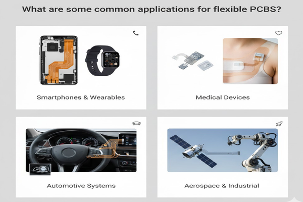
What are some common applications for flexible PCBs?
Where do we see flexible PCBs making a real difference in our daily lives? From the tiny devices we carry to complex industrial systems, their applications are vast and growing.
Flexible PCBs are essential in compact electronics like smartphones and wearables, medical devices, automotive systems, and aerospace applications due to their space-saving, durable, and adaptable properties. They enable smaller, more reliable, and more complex designs.
I remember working on a project where space was incredibly tight. A rigid PCB simply wouldn't fit. That's when flexible PCBs became a game-changer, and I truly understood their value.
Consumer Electronics
This is perhaps the most visible area for flexible PCBs. My smartphone, for example, is packed with them. They are used in cameras, displays, buttons, and connecting various modules. Wearable devices like smartwatches and fitness trackers heavily rely on flexible PCBs because they need to be small, light, and conform to the body's contours. Even modern laptops use them to connect the keyboard and touchpad.
Medical Devices
In the medical field, reliability and miniaturization are paramount. Flexible PCBs are found in implantable devices (like pacemakers), hearing aids, surgical tools, and diagnostic equipment. Their ability to bend and fit into small, irregular spaces, combined with their durability, makes them ideal for critical applications where failure is not an option.
Automotive Industry
Modern cars are increasingly electronic. Flexible PCBs are used in infotainment systems, LED lighting, dashboard displays, sensors, and engine control units. They can withstand vibrations, temperature fluctuations, and the harsh automotive environment while allowing for complex wiring in tight spaces. This makes vehicles safer and more connected.
Aerospace and Defense
For aircraft, satellites, and military equipment, weight reduction and reliability are crucial. Flexible PCBs are lighter and more compact than traditional wiring harnesses, reducing fuel consumption and increasing payload capacity. They are also highly durable, essential for systems operating in extreme conditions.
Industrial Applications
Flexible PCBs also serve in industrial settings, including robotics, automation systems, and test equipment. Their ability to withstand repeated movement and harsh operating conditions ensures long-term reliability in factories and other demanding environments.
| Application Sector | Examples of Devices/Uses | Key Benefit Utilized |
|---|---|---|
| Consumer Electronics | Smartphones, wearables, cameras, laptops | Miniaturization, space-saving, form factor freedom |
| Medical Devices | Pacemakers, hearing aids, surgical tools | Reliability, small size, biocompatibility |
| Automotive Industry | Dashboards, lighting, sensors, engine control | Durability (vibration/temp), complex wiring |
| Aerospace & Defense | Satellites, aircraft, military electronics | Weight reduction, high reliability, extreme environment |
| Industrial Applications | Robotics, automation, test equipment | Durability under movement, harsh conditions |
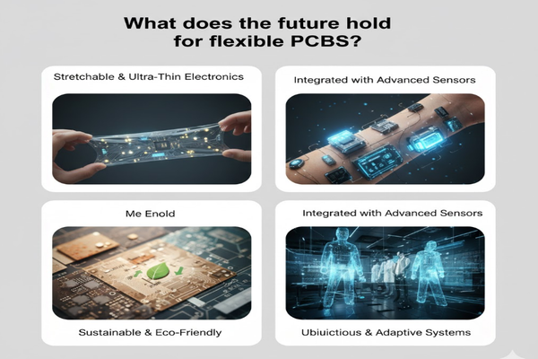
What does the future hold for flexible PCBs?
Considering their current impact, what advancements can we expect for flexible PCBs? The technology is still evolving rapidly, promising even more innovative applications.
The future of flexible PCBs includes further advancements in ultra-thin, stretchable electronics, integration with advanced sensors, and the adoption of more sustainable materials, opening doors for truly ubiquitous and adaptive electronic systems.
I believe the flexible PCB story is just beginning. As technology pushes boundaries, these bendable circuits will be at the forefront of innovation, shaping our future in exciting ways.
Ultra-Thin and Stretchable Electronics
The trend towards thinner and more flexible circuits will continue, leading to "flex-on-flex" and even stretchable electronics. This means PCBs that can not only bend but also stretch and conform to highly irregular, dynamic surfaces, like human skin. This will enable next-generation wearables, biomedical patches, and smart textiles.
Integration with Advanced Sensors
Flexible PCBs will increasingly integrate more sophisticated sensors directly into their structure. Imagine smart bandages that monitor vital signs and deliver medicine, or flexible robotic skins with tactile feedback. This will create highly functional and adaptive systems in compact, flexible packages.
Sustainable and Biodegradable Materials
As environmental concerns grow, there will be a push for more eco-friendly flexible PCB materials. Researchers are exploring biodegradable substrates and lead-free manufacturing processes to reduce the environmental footprint of electronics. This will be a crucial step towards a greener electronics industry.
Roll-to-Roll Manufacturing
To drive down costs and increase production volume, roll-to-roll (R2R) manufacturing techniques will become more prevalent. This method, similar to printing newspapers, allows for continuous, high-volume production of flexible circuits on a roll of substrate, making them more accessible for a wider range of applications.
3D Flexible Circuits
Beyond traditional 2D flexible circuits, the future will see more complex 3D flexible circuits that can fold and form intricate shapes, creating true three-dimensional electronic structures. This will enable even greater space savings and novel device architectures.
| Future Trend | Description | Potential Impact |
|---|---|---|
| Ultra-Thin/Stretchable | PCBs that can bend, stretch, and conform dynamically | Next-gen wearables, biomedical patches, smart textiles |
| Advanced Sensor Integration | Embedding sophisticated sensors directly into the circuit | Smart bandages, flexible robotic skins |
| Sustainable Materials | Use of biodegradable substrates, eco-friendly processes | Reduced environmental impact of electronics |
| Roll-to-Roll Manufacturing | Continuous, high-volume production on rolls | Lower costs, wider adoption, increased accessibility |
| 3D Flexible Circuits | Complex folding and forming into intricate 3D structures | Greater space savings, novel device architectures |
Conclusion
Flexible PCBs are truly amazing, revolutionizing electronics by making devices smaller, lighter, and more reliable. Their ability to bend and fit makes them essential in our modern world.

