
Ever wonder how the green boards inside your electronics come to life? Printed Circuit Boards (PCBs) are vital, but their creation is complex.
Understanding the PCB manufacturing process[^1] helps you appreciate the hidden technology that powers our world. It ensures devices work right.
Join me as I pull back the curtain on PCB manufacturing. We'll explore each critical step, from initial design to the final, functional board. Knowing this process helps you make better choices for your projects.
What Are the Key PCB Manufacturing Process Steps?
Are you curious about the journey a PCB takes from an idea to a tangible component? The manufacturing process is a precise series of steps, each vital for a functional board.
Each step in PCB manufacturing is like building blocks. They layer up to create a reliable and efficient electronic foundation.
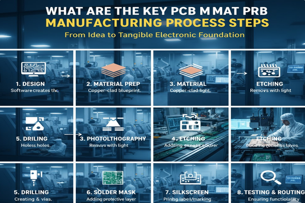
Let's break down the essential stages I've encountered in my experience. I'll explain how each part contributes to the final product.
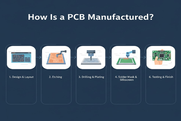
Design and Layout: The Blueprint Stage
The process begins long before any physical board exists. It starts with design and layout[^2]. This is where engineers create the exact blueprint for the PCB. They decide where every component goes and how all the traces connect. This stage sets the foundation for everything that follows. It impacts performance and manufacturability.
| Design Aspect | Description | Importance |
|---|---|---|
| Schematic Capture | Translating circuit idea into symbols. | Defines electrical connections. |
| Component Placement | Positioning parts on the board. | Affects signal integrity and heat. |
| Routing | Drawing traces (copper paths). | Connects components; must avoid shorts. |
| DRC (Design Rule Check) | Verifying design against manufacturing limits. | Prevents errors before production. |
Copper Layer Structuring: Building the Paths
Once the design is ready, we move to structuring the copper layers. This involves preparing the core material, usually fiberglass, and adding copper foil. The copper will later become the electrical pathways. This step is about precise layering. It ensures good adhesion between materials. This process involves cleaning and pre-treating the base laminate to ensure optimal bonding. Different types of copper foil thickness are chosen based on the final current requirements of the PCB. We ensure the copper is evenly applied across the entire surface. This lays the groundwork for accurate circuit etching.
Etching and Lamination: Shaping the Circuits
After layering, etching removes unwanted copper. This leaves only the designed traces and pads. Then, lamination presses multiple layers together under heat and pressure. This creates a solid, multi-layered board. This is where the circuit patterns truly emerge. Photolithography creates the circuit pattern by exposing photosensitive resist to UV light. Chemical etchants then remove the unprotected copper. For multi-layer boards, individual layers are etched and then precisely aligned and bonded together using heat and pressure with prepreg materials. This forms a single, integrated board structure.
Drilling and Plating: Making Connections
Next, drilling creates holes for components and connections between layers. After drilling, a plating process deposits a thin layer of copper inside these holes. This ensures electrical continuity through the board. This step is crucial for multi-layer PCBs. High-speed drills or lasers create precise holes for vias and component leads. The drilled holes are then chemically cleaned. An electroless copper deposition process coats the hole walls, followed by electrolytic plating to thicken the copper. This establishes robust electrical connections between different layers of the PCB.
Inspection and Quality Control: Ensuring Perfection
Quality control is ongoing, but a dedicated inspection phase checks for defects. This includes automated optical inspection (AOI) and electrical tests. It catches errors early. This stage guarantees the board meets design specifications. It prevents costly failures later on. Automated Optical Inspection (AOI)[^3] systems scan the boards for flaws like shorts, opens, or missing features by comparing them to the design files. Electrical tests (E-test) verify continuity and isolation. X-ray inspection[^4] is used for internal layers on complex boards. My team rigorously checks each batch to ensure every board adheres to the strict quality parameters we set.
Final Assembly and Finishing: The Complete Board
The final step involves adding a solder mask[^5] (the green coating) and silkscreen (component labels). Surface finishes are applied to improve solderability and protect the copper. Then, components are assembled onto the board. This makes it ready for its intended use. A solder mask protects the copper traces from oxidation and prevents solder bridges during assembly. The silkscreen adds labels for components and polarity, aiding assembly and troubleshooting. Various surface finishes like ENIG (Electroless Nickel Immersion Gold) or HASL (Hot Air Solder Leveling) are applied to ensure good solderability and corrosion resistance. Finally, the boards are cut to their final size and packaged for delivery.
How Can I Ensure the Quality and Reliability of My PCBs?
Worried about your PCBs failing prematurely or not performing as expected? Quality and reliability are not accidental; they are built into the manufacturing process.
Guaranteeing top-notch PCBs means paying close attention to every detail, from design to final testing. It stops problems before they start.
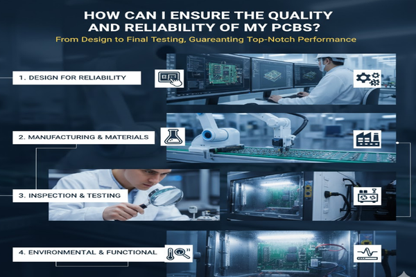
I've learned that consistent quality comes from rigorous checks and adherence to standards. Let me share how I ensure PCBs stand the test of time.
Material Selection: The Foundation of Durability
The materials chosen for a PCB greatly impact its reliability. Different applications require different substrates, copper types, and finishes. Using the correct materials ensures the board can withstand its operating environment. It also affects its electrical performance. For instance, high-frequency applications[^6] demand materials with low dielectric loss, while high-power devices need materials with excellent thermal management properties. I always evaluate the end-use environment, including temperature ranges, humidity, and mechanical stress, to select the most appropriate laminate and surface finish. This careful selection prevents issues like delamination or trace degradation.
| Material Type | Key Characteristics | Impact on Quality |
|---|---|---|
| FR-4 (Standard) | Cost-effective, good electrical properties. | Suitable for general use. |
| High-Tg Materials | Withstands higher temperatures. | Essential for high-power devices. |
| Flexible Materials | Bends without breaking. | Critical for flexible electronics. |
| Surface Finish (ENIG, HASL) | Protects copper, aids soldering. | Affects solder joint reliability. |
Process Control: Consistency is Key
Strict process control at every manufacturing stage minimizes variations and defects. This involves precise temperature, pressure, and chemical concentration management. Consistent process parameters lead to consistent product quality. Deviations can introduce weaknesses. We employ statistical process control (SPC) to monitor critical parameters throughout production. This includes monitoring plating bath concentrations, etching times, and lamination cycles. Regular calibration of machinery and environmental controls, like cleanroom conditions, further ensures stability. My team diligently tracks these metrics, making real-time adjustments to maintain uniformity across all batches.
Testing and Validation: Proving Performance
Extensive testing and validation are non-negotiable for reliable PCBs. This includes electrical testing, functional testing, and environmental testing. These tests simulate real-world conditions. They confirm the board will perform as expected over its lifespan. Automated optical inspection (AOI) meticulously checks for visual defects. Electrical tests (E-test) verify every net for opens and shorts. Beyond these, we conduct stress tests, such as thermal cycling and humidity exposure, to simulate harsh operating conditions. This proactive testing identifies potential failure points before boards reach the customer, ensuring robust performance.
- Automated Optical Inspection (AOI): Scans boards for visual defects like shorts or open circuits.
- Electrical Test (E-test): Checks continuity and isolation between connections.
- X-ray Inspection: Used for complex multi-layer boards to check internal connections.
- Environmental Testing: Exposes boards to temperature extremes, humidity, and vibration.
Need Someone to Manufacture Your PCB? south-electronic can help!
Struggling to find a reliable partner to bring your PCB designs to life? A trustworthy manufacturer is crucial for high-quality, dependable boards.
Choosing the right manufacturing partner can save you time, money, and headaches. They turn your ideas into working products.
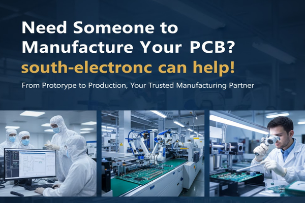
I've seen firsthand the difference a good manufacturing partner makes. south-electronic offers expertise and dedication to precision. They can be your solution.
Expertise and Experience: A Proven Track Record
south-electronic has a strong background in PCB manufacturing. We bring years of experience to every project. Our team understands the nuances of various PCB types. We handle everything from simple single-layer boards to complex multi-layer designs. This expertise ensures your project is in capable hands. Our engineers possess deep knowledge of DFM (Design for Manufacturability) principles, offering valuable feedback to optimize your designs for production efficiency and cost-effectiveness. We stay updated with the latest industry standards and technologies. This allows us to tackle even the most demanding PCB challenges, ensuring a smooth transition from concept to reality.
| Aspect of Expertise | Description | Benefit to You |
|---|---|---|
| Design Review | Catching potential manufacturing issues early. | Reduces rework and costs. |
| Material Sourcing | Access to quality materials for specific needs. | Ensures board performance and longevity. |
| Advanced Techniques | Ability to handle complex geometries and fine traces. | Supports innovative designs. |
| Troubleshooting | Resolving unexpected issues efficiently. | Minimizes delays in production. |
Quality Assurance: Our Commitment to Excellence
Our commitment to quality is unwavering. We implement stringent quality control measures at every step of the manufacturing process. This includes thorough inspections and comprehensive testing. We ensure every PCB meets the highest industry standards. We aim for zero defects. From initial material inspection upon arrival to final electrical and functional tests before shipment, every board undergoes rigorous checks. We adhere to international quality certifications, such as ISO 9001[^7], to maintain consistent processes. This meticulous approach guarantees that the PCBs you receive are reliable and perform exactly as intended.
Customer Support: Your Partner in Success
At south-electronic, we believe in strong partnerships. We offer excellent customer support throughout your project. From initial consultation to post-production assistance, we are here for you. We communicate clearly and respond quickly to your needs. Your success is our priority. We assign a dedicated project manager to each client, ensuring a single point of contact for all your inquiries. Our team is available to provide technical support and guidance, addressing any concerns promptly. We pride ourselves on transparent communication and proactive updates, keeping you informed at every stage of your PCB manufacturing journey.
Conclusion
The PCB manufacturing process is detailed and complex. Understanding it ensures high-quality electronic devices.
[^1]: Learn about the intricate steps involved in PCB manufacturing and their impact on device performance. [^2]: Discover how the initial design phase influences the functionality and reliability of PCBs. [^3]: Find out how AOI technology enhances defect detection in PCB production. [^4]: Discover how X-ray technology helps in inspecting complex multi-layer PCBs. [^5]: Discover how solder masks protect PCBs and enhance their performance during assembly. [^6]: Explore the materials that ensure optimal performance in high-frequency PCB designs. [^7]: Understand the importance of ISO 9001 certification in ensuring quality in PCB production.

