

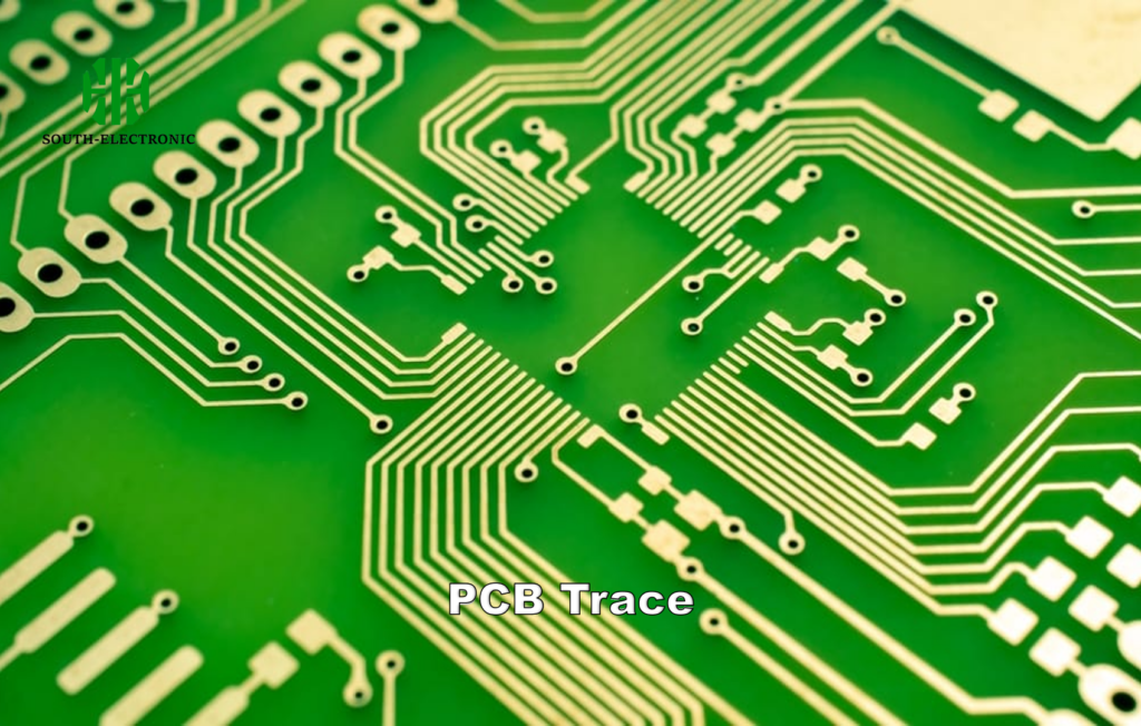
PCBs are susceptible to pad damage during manufacturing or rework, where pads can become damaged or completely detach from the board. This can render the PCB unusable because components cannot be properly soldered.
Pad repair allows you to repair defects without scrapping the entire PCB. However, all pad repairs should be performed with caution, as they can affect long-term reliability if not performed properly. Don’t worry, Jiepei will show you how to bring these damaged PCBs back from the brink of death and give your electronic devices a new lease of life!
Pad damage can be caused by a variety of factors, including overheating, mechanical damage, manufacturing defects, corrosion, handling damage, and repeated rework. These factors can all cause pads to become detached or damaged, compromising the PCB’s function.
Repair Tip 1: Copper Foil Chipping
First, we can use copper foil chipping. This is a low-cost, easy-to-use method suitable for repairing outer layer pads. Simply apply small squares of copper foil to the damaged area and secure with epoxy. However, be aware that the reliability of this method is limited by the strength of the epoxy.

Repair Tip 2: Copper Tape Patching
If you need to repair wider pads, copper tape patching is a good option. Covering the damaged area with conductive copper tape and then covering it with non-conductive Kapton tape improves reliability, especially during rework.
Repair Tip 3: Circuit Frame
The circuit frame technique is suitable for situations where a sealing epoxy repair material is required. An insulating frame is bonded around the damaged pad and then filled with conductive epoxy. This method allows repairs on pads of any size.
Repair Tip 4: Conformal Coating
Conformal coating is particularly important when space around the pad is limited. Covering the damaged area with an insulating acrylic coating and then applying a conductive coating to rebuild the pad is a simple and effective method.

Repair Tip 5: Solder Mask Bridge
The solder mask bridge technique is suitable for situations where a portion of the pad has fallen off. Using solder mask to bridge the gap between the broken pad segments and then electrically rebuilding the pad provides a reliable repair.
Repair Tip 6: Epoxy Fill
Epoxy fill is a method that allows repairs without modifying the pad geometry. Conductive epoxy is injected under the pad to reattach it, but this method requires significant process expertise.
Repair Tip 7: Trace Bridge Jumper
For small pad gaps, trace bridge jumper is a simple and effective method. Soldering a thin insulated wire between the disconnected pad segments is done with limited space, but be aware that bending the wires may affect long-term reliability.
Repair Tip 8: PCB Rework
Finally, for multilayer boards, PCB rework techniques can be used. Layers are stripped back to expose the inner pads, the pads are repaired, and the board is rebuilt. This is a highly complex method suitable for PCBs that are very expensive and cannot be remanufactured. For more information, please contact Jiepei.

