

Getting your PCB design ready is only step one. If you don’t know how production works, delays and defective boards could kill your project. Mastering the process saves money and avoids headaches.
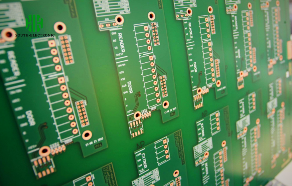
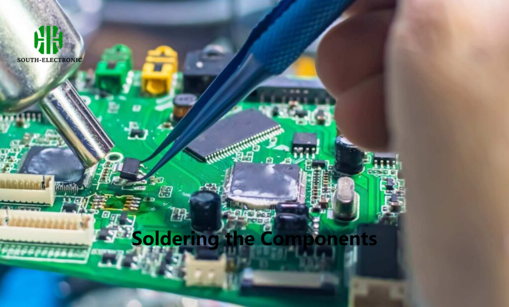
PCB production involves designing, fabricating, and assembling boards. It starts with your Gerber/ODB++ files, then layers get etched, laminated, drilled, plated, and finished with solder mask/silkscreen – creating functional electronics step by step.
Knowing these basics is crucial. But let’s explore the details affecting your project timelines, costs, and quality next.
How long does it take to manufacture a PCB?
Waiting for boards delays everything. Rush orders cost extra while standard timelines feel slow. Smart planning cuts waiting time without overspending.
Standard PCB production takes 5–15 days: 1–3 days for file checks, 3–7 days for fabrication, 1–3 days for assembly. Prototype PCB production can be fastest in 24 hours. Rush services cost 20–50% more but skip queues.

Breaking down production stages
Lead time varies by complexity and vendor location. Prototype pcb production is quickest for small batches. Full industrial pcb production stretches longer. I once panicked when my IoT prototype stalled. Splitting orders saved me: basic boards from a cheap pcb production service first, complex ones later.
Key factors affecting duration:
| Factor | Impact on Time | Example |
|---|---|---|
| Layer count | +2–4 days per layer | 4-layer vs. 8-layer flex pcb |
| Surface finish | +1 day | HASL vs. ENIG |
| Testing depth | +1–3 days | Basic vs. 100% AOI inspection |
| Shipping origin | +3–7 days | China vs. pcb production usa |
Optimize by finalizing designs early and confirming vendor schedules. Off-peak seasons like late autumn speed things up. For fast custom pcb production, pay extra for expedited materials handling. Budget 30% time buffer for revisions.
USA vs. China for PCB Production: Where Should You Manufacture Your Boards?
Choosing a production location feels overwhelming. China offers big savings but shipping takes weeks. US shops are closer yet pricier. Your project needs decide what trade-offs work.
China excels in cost and scale: basic 4-layer boards cost 70% less than US options with 10,000+ unit discounts. pcb production usa offers faster shipping (2–5 days), IP safety, and easier revisions. Custom pcb production benefits from US communication.

Comparing location trade-offs
I once faced customs delays from Shenzhen, pushing my launch back. Now I differentiate: prototypes stay domestic, bulk orders go overseas for cheap pcb production. pcb production china dominates in tooling and machinery for complex runs but lags in quick-turn jobs.
Breakdown of key differences:
| Criteria | China Advantage | USA Advantage |
|---|---|---|
| Cost | $0.05 per sq. inch (volume) | $0.20 per sq. inch |
| Lead time | Slower (7–15 days + shipping) | Faster (3–7 days locally) |
| Quality | Good with tier-1 suppliers | Consistent, strict IPC-6012 |
| Communication | Time-zone challenges | English support 24/7 |
China wins for simple pcb printing at massive volumes. Use US partners for urgent prototype pcb production or complex flex pcb designs needing tight oversight. Ask vendors about their pcb production machine capabilities. Hybrid sourcing balances costs and risks effectively.
How PCB Production Cost is Calculated (And How to Optimize Yours)?
Seeing quotes shock newcomers. Hidden fees from material waste or design tweaks inflate budgets fast. Knowing cost drivers saves hundreds per batch.
PCB cost depends on size, layers, materials, finishes, and labor. A 100-unit order might be $2–$10 per board. Optimize using standard sizes, fewer layers, ENIG finishes only where needed, and panelization to reduce waste.
Slashing expenses strategically
My first prototype pcb production cost doubled due to unnecessary gold plating. Now I specify finishes per area. Cheap pcb production isn’t about low quality but process efficiency. pcb production process waste adds up silently in scrap rates.
Cost calculation factors:
| Component | Price Influence | Optimization Tip |
|---|---|---|
| Board size | High (material usage) | Fit multiple designs in one panel |
| Layer count | Very high | Cut inner layers if possible |
| Hole density | Moderate (drilling time) | Use larger via sizes |
| Surface finish | High | Selective ENIG instead of all-over |
| Testing | Low–moderate | Skip full AOI for prototypes |
Order in bulk during pcb production china sales. For US needs, negotiate with pcb production service firms on slower delivery discounts. Avoid flexible boards unless required. Partner with factories directly for recurring custom pcb production to lock rates.
Conclusion
Understanding pcb board production steps, timelines, vendor options, and costs ensures smoother projects. Apply these insights to cut expenses and delays effectively.

