
Ever wondered how the circuit boards inside your gadgets come to life? The journey from a raw design to a functional PCB is intricate.
PCB manufacturing[^1] involves a precise, multi-step process, transforming raw materials into the vital interconnected pathways that power our electronics, ensuring components communicate seamlessly for optimal device performance.
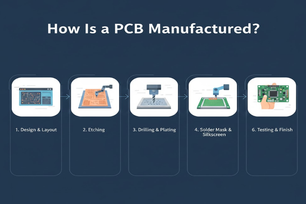
Understanding the manufacturing process of a Printed Circuit Board[^2] (PCB) offers a fascinating look into the heart of modern electronics. Let's peel back the layers and discover how these essential components are made, step by step.
What Are the Step-by-Step PCB Manufacturing Processes?
Frustrated by electronics that don't work as expected? The quality of a PCB directly impacts device reliability.
The PCB manufacturing process involves several critical stages, including design, etching, drilling, and quality control, each crucial for creating a robust and reliable circuit board that meets specific electronic requirements.

Conception et implantation (Design and Layout)
This initial phase is where the entire PCB journey begins. It’s not just about drawing lines; it's about translating an electronic circuit diagram into a physical layout. I always start here, ensuring every component has its place and every trace connects correctly.
Structuration des couches de cuivre (Copper Layer Structuring[^3])
Once the design is solid, we move to shaping the copper. This step involves applying a photolithographic mask to a copper-clad laminate, exposing it to UV light, and then developing it. It’s like creating a stencil for the electrical pathways.
Gravure et lamination (Etching and Lamination[^4])
After structuring, unwanted copper is removed through etching, leaving only the desired circuit traces. For multi-layer PCBs, lamination bonds these individual layers together under high pressure and temperature, creating a single, integrated board.
Perçage et cuivrage (Drilling and Copper Plating[^5])
Holes are drilled for components and for connecting different layers. These holes are then plated with copper to ensure electrical conductivity between layers. This is a critical step for creating vertical connections.
Inspection et contrôle qualité (Inspection and Quality Control[^6])
No PCB leaves the factory without rigorous checks. Automated optical inspection (AOI) and electrical tests ensure that every trace is perfect and every connection works. This is where we catch any flaws before they become bigger problems.
Assemblage et conditionnement final (Assembly and Final Packaging[^7])
Finally, components are mounted onto the PCB, either through surface-mount technology (SMT) or through-hole methods. The finished boards are then cleaned, tested again, and packaged, ready for integration into electronic devices.
What Are the Common PCB Types and Special Technologies?
Confused by all the different PCB types out there? Choosing the right board is key to your project’s success.
Common PCB types include single-sided, double-sided, and multi-layer boards, while special technologies like flexible, rigid-flex, and HDI PCBs offer advanced solutions for complex electronic designs.

When I first started, I thought a PCB was just a PCB. I quickly learned there’s a whole world of options, each suited for different applications.
Types of PCBs
| Type | Description | Common Use Cases |
|---|---|---|
| Single-Sided | One layer of conductive material. | Simple electronics, power supplies |
| Double-Sided | Two layers of conductive material with through-hole connections. | Consumer electronics, industrial control |
| Multi-Layer | More than two layers, stacked and interconnected. | Complex devices, computers, servers |
Special Technologies
Flexible PCBs[^8]
These boards can bend and flex, making them ideal for devices that require dynamic movement or compact spaces. I’ve used them in wearables and specialized medical equipment, where rigid boards simply wouldn't fit.
Rigid-Flex PCBs[^9]
Combining rigid and flexible sections, these PCBs offer the best of both worlds. They reduce the need for connectors, improving reliability and saving space in applications like cameras and aerospace.
High-Density Interconnect (HDI) PCBs[^10]
HDI PCBs feature finer lines, smaller vias, and higher connection pad density. They are essential for miniaturization and high-performance devices, allowing more components in a smaller area. Think smartphones and high-end computing.
What Are the Challenges in PCB Manufacturing?
Worried about your PCB project running into roadblocks? Manufacturing PCBs is not always straightforward.
PCB manufacturing faces challenges such as managing design complexity, ensuring material quality, maintaining precise tolerances, and controlling costs, all while adhering to strict environmental regulations and tight production schedules.

I’ve seen projects delayed and budgets overrun due to unforeseen manufacturing hurdles. It’s crucial to be aware of these challenges.
Design Complexity
Modern electronics demand increasingly complex PCB designs. High-speed signals, dense component placement, and multi-layer structures create significant design challenges. Ensuring signal integrity and power delivery across these complex layouts is a constant battle. I spend hours optimizing layouts to avoid issues down the line.
Material Quality and Sourcing[^11]
The quality of raw materials directly impacts the final PCB's performance and reliability. Sourcing consistent, high-quality copper laminates, prepregs, and soldermasks from reliable suppliers can be a challenge, especially with global supply chain disruptions. I always verify material certifications.
Precision and Tolerances[^12]
PCB manufacturing requires incredible precision. Etching fine lines, drilling tiny holes, and aligning multiple layers demand advanced machinery and strict process control. Even a slight deviation can lead to defects, requiring rework or rejection. Maintaining tight tolerances across large production runs is a significant technical feat.
Cost Control[^13]
Balancing quality with cost is always a delicate act. The cost of materials, specialized equipment, labor, and rigorous testing can add up quickly. Optimizing production processes to reduce waste and improve efficiency without compromising quality is a continuous challenge for manufacturers.
Environmental Regulations[^14]
The chemicals used in PCB manufacturing, especially during etching and plating, can be hazardous. Manufacturers must comply with strict environmental regulations for waste disposal and emissions. Adopt greener technologies and sustainable practices is a growing imperative and a complex undertaking.
How to Find the Best PCB Manufacturer for Your Needs?
Struggling to pick the right PCB partner? Your choice of manufacturer can make or break your product.
Finding the best PCB manufacturer requires evaluating their expertise, quality certifications, technological capabilities, customer service, and pricing to ensure they align with your project's specific requirements and budget.

I’ve learned the hard way that not all manufacturers are created equal. Here’s what I look for to ensure a smooth project.
Expertise and Experience
Look for manufacturers with a proven track record in producing PCBs similar to your requirements. Do they specialize in high-frequency, flexible, or HDI boards if your project needs them? Their experience often translates to fewer issues and higher quality. I always ask for case studies or examples of their work.
Quality Certifications
Certifications like ISO 9001 (quality management) and ISO 14001 (environmental management) indicate a commitment to quality and responsible practices. UL certification is also crucial for safety standards. These certifications give me peace of mind that their processes are rigorously controlled.
Technological Capabilities
Assess their equipment and capabilities. Can they handle the complexity of your design, including specific layer counts, trace widths, and material types? Advanced fabrication equipment and testing facilities are signs of a capable manufacturer. I make sure they can meet my most demanding specifications.
Customer Service and Communication
Clear and prompt communication is vital, especially when issues arise. A good manufacturer will offer dedicated support, provide regular updates, and be proactive in addressing concerns. I value a partner who is transparent and responsive.
Pricing and Lead Times
While cost isn't the only factor, it's important. Get detailed quotes and compare pricing structures. Also, consider their typical lead times for prototypes and production runs. A balance between competitive pricing and realistic lead times is often the sweet spot.
Conclusion
Manufacturing a PCB is a complex dance of design and precision. Understanding each step helps us appreciate the technology powering our world.
[^1]: Explore this resource to understand the intricate steps involved in PCB manufacturing and how they impact electronics. [^2]: Learn about the significance of PCBs in electronics and their manufacturing process. [^3]: Understand the importance of copper layer structuring in creating effective circuit pathways. [^4]: Explore the etching and lamination process to see how PCBs are formed. [^5]: Learn how drilling and copper plating ensure electrical connectivity in PCBs. [^6]: Find out how rigorous inspection processes ensure the reliability of PCBs. [^7]: Discover the final steps in PCB production and their importance for product readiness. [^8]: Learn about the advantages of flexible PCBs in modern electronics. [^9]: Discover how Rigid-Flex PCBs combine flexibility and rigidity for innovative designs. [^10]: Understand the significance of HDI PCBs in miniaturization and high-performance devices. [^11]: Explore the impact of material quality on PCB performance and reliability. [^12]: Learn how precision affects the quality and functionality of PCBs. [^13]: Discover the balance between quality and cost in PCB production. [^14]: Understand the importance of adhering to environmental regulations in PCB production.

