
Ever wondered how the green boards inside your electronics come to life? The journey from a raw idea to a functional PCB is fascinating and complex.
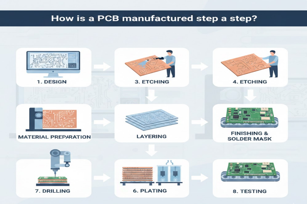
PCB manufacturing involves a precise multi-step process, beginning with design and material preparation[^1], followed by etching[^2], layering[^3], drilling[^4], plating[^5], and finishing[^6], culminating in a robust circuit board ready for components.
Understanding this intricate dance of technology and precision reveals the magic behind every electronic device we use. Stick with me as we uncover the secrets of how these essential components are made.
How long does it take to manufacture a PCB?
Impatience is common, especially when waiting for a crucial component. How long until your custom PCB is ready for action?
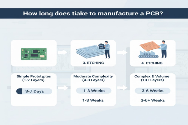
PCB manufacturing time varies significantly based on complexity, layers, quantity, and specific technologies, typically ranging from a few days for simple prototypes to several weeks for complex, high-volume orders.
The timeline for PCB manufacturing is not a fixed number; it depends on several key factors. My experience tells me that prototyping can be surprisingly fast, sometimes just a few days if you use a quick-turn service. However, large production runs with intricate designs demand more time.
Factors Affecting PCB Manufacturing Time
| Factor | Impact on Timeline |
|---|---|
| Design Complexity | More layers, finer traces, and tighter tolerances increase production time. |
| Material Type | Exotic materials or specific dielectric constants may require special handling and procurement time. |
| Quantity | Larger orders naturally take longer due to increased processing and quality control steps. |
| Technology | Advanced technologies like HDI (High-Density Interconnect) or flexible PCBs add to the manufacturing duration. |
| Testing Regimen | Extensive testing and certification processes prolong the overall schedule. |
| Supplier Load | The manufacturer's current workload can also influence lead times. |
For instance, a standard two-layer board might ship in 5-7 business days, while an 8-layer board with blind/buried vias could take 15-20 business days. Expedited options exist but always come at a premium. It's always a balance between speed, cost, and quality.
What are the raw materials for PCB manufacturing?
Before any circuits can form, what are the fundamental ingredients that make up a PCB? It all starts with the right materials.
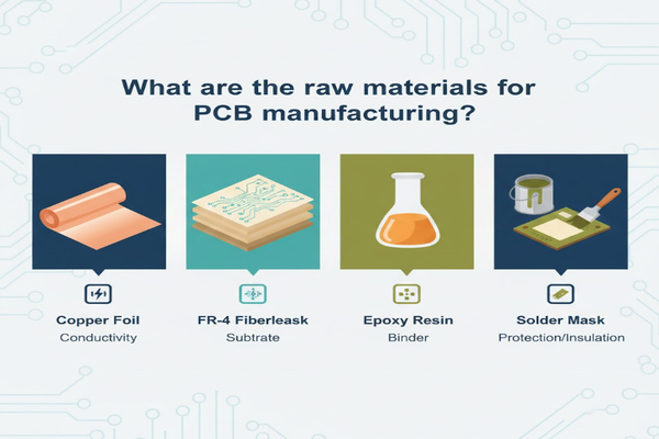
Key raw materials for PCB manufacturing include copper foil for conductivity, fiberglass (FR-4) for the substrate, epoxy resin as a binder, and solder mask[^7] for protection and insulation.
Dive deeper Paragraph: The foundation of any PCB lies in its raw materials. Without these, the sophisticated electronic pathways simply wouldn't exist. When I first learned about PCB fabrication, I was surprised by the relatively simple yet incredibly functional components involved.
Essential PCB Raw Materials
| Material | Primary Function | Characteristics |
|---|---|---|
| Substrate (FR-4) | Provides mechanical support and electrical insulation. | Flame retardant, good strength-to-weight ratio, common. |
| Copper Foil | Forms the conductive traces and planes. | Excellent electrical conductivity, easily etched. |
| Prepreg | Acts as an adhesive and insulating layer between core materials. | Resin-impregnated glass fiber, cures under heat and pressure. |
| Solder Mask | Protects copper traces from oxidation and short circuits. | Green, blue, red, or black polymer coating. |
| Silkscreen Ink | Used for component designators and markings. | Non-conductive, applied via screen printing. |
| Drill Bits | Create holes for vias and component leads. | Tungsten carbide, very precise and durable. |
| Etching Chemicals | Remove unwanted copper during circuit definition. | Ferric chloride or cupric chloride solutions. |
The combination of these materials, especially the precise layering of copper and fiberglass, is what allows for the creation of multi-layered boards that power our most advanced electronics.
What are the 7 types of PCB testing methods?
After all the hard work of manufacturing, how do we ensure a PCB actually works? Testing is the crucial final step to guarantee reliability.
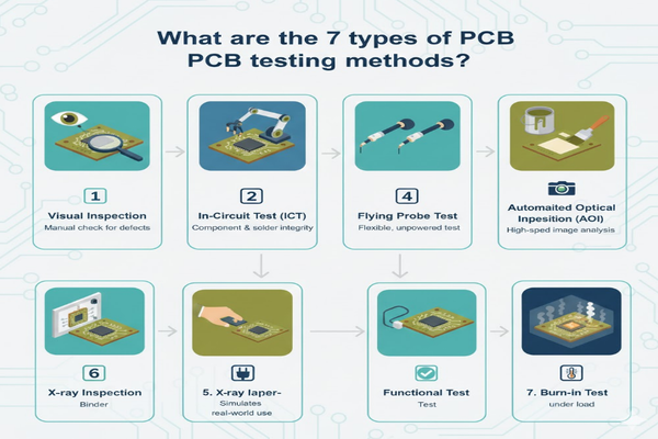
PCB testing methods[^8] include Visual Inspection[^9], In-Circuit Test (ICT)[^10], Flying Probe Test, Automated Optical Inspection (AOI)[^11], X-ray Inspection, Functional Test, and Burn-in Test[^12], each ensuring quality and performance.
Ensuring a PCB is fully functional and reliable is paramount. My experience in product development has shown me that skipping or inadequately performing these tests can lead to costly failures down the line. It's not just about seeing if it turns on; it's about verifying every connection and component.
Common PCB Testing Methodologies
| Testing Method | Description | Purpose |
|---|---|---|
| Visual Inspection | Manual or automated examination for obvious defects like shorts, opens, or misaligned components. | Identifies gross manufacturing errors and cosmetic flaws. |
| In-Circuit Test (ICT) | Uses a bed-of-nails fixture to check individual components and connections. | Verifies correct component placement, shorts, opens, and component values. |
| Flying Probe Test | Robotic probes move across the board to test points without a fixture. | Cost-effective for prototypes and low-volume production; checks shorts, opens, and resistance. |
| Automated Optical Inspection (AOI) | High-resolution cameras scan the board for defects by comparing it to a known good image. | Detects missing components, polarity issues, solder bridging, and trace defects. |
| X-ray Inspection | Penetrates components to inspect hidden solder joints, especially for BGAs and QFNs. | Uncovers internal defects, voids, and misalignments in complex packages. |
| Functional Test | Simulates the PCB's intended operating environment. | Confirms the board performs its intended electronic functions correctly. |
| Burn-in Test | Subjects the PCB to extreme temperature and voltage for an extended period. | Accelerates potential early failures, ensuring long-term reliability. |
Each method plays a critical role in catching different types of defects, ensuring that the final PCB is robust and meets all design specifications before it's integrated into a final product.
Conclusion
From raw materials to rigorous testing, PCB manufacturing is a marvel of precision engineering, ensuring our electronic world functions flawlessly.
[^1]: Learn about the crucial first steps in PCB manufacturing that set the foundation for quality. [^2]: Discover how etching shapes the conductive pathways on a PCB, a key step in the manufacturing process. [^3]: Understand how layering contributes to the complexity and functionality of modern PCBs. [^4]: Find out how drilling creates necessary holes for components and connections in PCBs. [^5]: Explore the importance of plating in enhancing conductivity and durability of PCBs. [^6]: Learn about the final touches that ensure a PCB is ready for use in electronic devices. [^7]: Learn how solder mask protects PCBs and enhances their performance in electronic applications. [^8]: Discover the various testing methods used to ensure the reliability and functionality of PCBs. [^9]: Understand the importance of Visual Inspection in identifying defects during PCB manufacturing. [^10]: Learn how ICT verifies the functionality of individual components on a PCB. [^11]: Explore how AOI technology enhances the quality control process in PCB manufacturing. [^12]: Find out how the Burn-in Test ensures long-term reliability of PCBs under stress conditions.

