
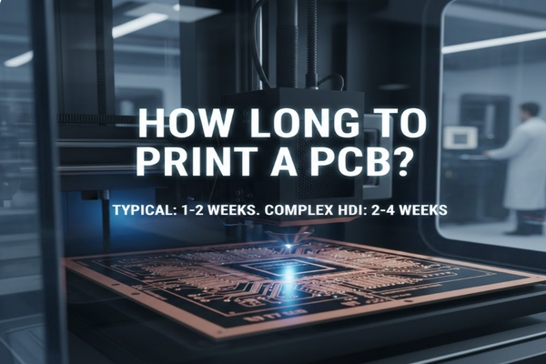
Struggling with project deadlines? The waiting game for PCB manufacturing can be a real headache.
For typical multilayer PCBs[^1], production usually takes one to two weeks. Complex HDI boards[^2] often need two to four weeks.
I know the frustration of tight schedules. Understanding PCB lead times helps you plan better and avoid costly delays. Let's explore the process.
How Does PCB Printing Work?
Ever wondered what goes into making those green circuit boards? It's a precise, multi-step process that demands attention to detail.
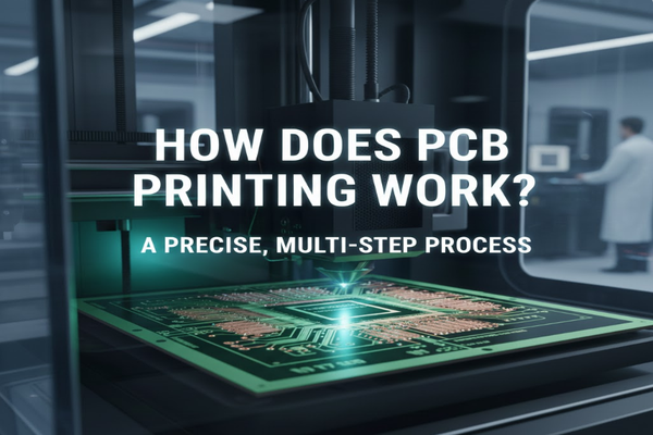
PCB printing, also known as PCB fabrication, involves transforming a digital design into a physical circuit board. This process includes imaging, etching, drilling, and plating, among other steps, creating the conductive pathways and connections needed for electronic components.
The PCB manufacturing process is a marvel of engineering, combining chemistry, optics, and precision mechanics. First, the design files are reviewed. This ensures manufacturability. Then, an inner layer image is transferred to copper-clad laminate using photoresist and UV light. Unwanted copper is etched away. Layers are then laminated together under heat and pressure. After lamination, holes are drilled for components and vias. A crucial step is electroplating, which deposits copper onto the hole walls to create conductive paths between layers. Outer layers are then imaged and etched. Finally, a solder mask[^3] is applied to protect the copper, and silkscreen printing adds component designators. Electrical testing checks for shorts and opens. This ensures every board functions as designed. The entire sequence requires careful control to maintain quality.
| Step | Description | Purpose |
|---|---|---|
| Design Review | Checking Gerber files and specifications | Ensure manufacturability |
| Inner Layer Prep | Imaging and etching inner copper layers | Create internal circuits |
| Lamination | Bonding layers with heat and pressure | Form a multi-layer board |
| Drilling | Creating holes for components and vias | Allow interconnections |
| Electroplating | Depositing copper in holes and on surfaces | Make holes conductive |
| Outer Layer Prep | Imaging and etching outer copper layers | Create external circuits |
| Solder Mask | Applying protective resin | Prevent short circuits, aid soldering |
| Silkscreen | Printing component labels and logos | Guide assembly |
| Electrical Test | Verifying circuit continuity and isolation | Ensure functionality |
| Final Finish | Applying surface finishes (e.g., ENIG, HASL) | Protect copper, improve solderability |
How to Avoid Common PCB Printing Mistakes?
Are you tired of costly re-spins and project delays due to preventable errors? Careful planning can make a huge difference.
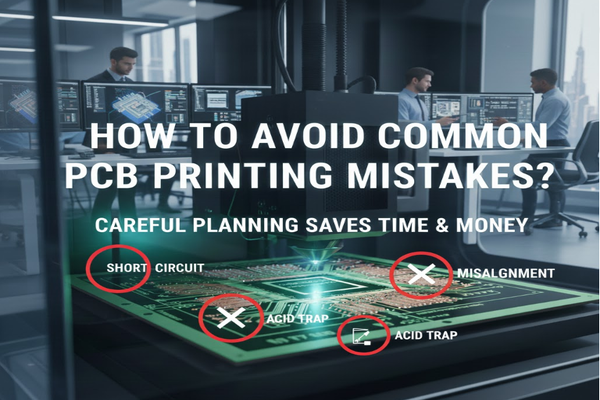
Avoiding common PCB printing mistakes involves thorough design review, clear communication with your manufacturer, and understanding material limitations, which together minimize errors and reduce overall project time and cost.
Many PCB manufacturing issues stem from design flaws or miscommunication. One key mistake is not adhering to manufacturer design rules. Each fabricator has specific tolerances for trace width[^4], spacing, drill sizes, and annular rings. Ignoring these leads to rejection or faulty boards. Another common error is inadequate panelization[^5]. If your board isn't properly panelized for production, it can increase costs and waste. Material selection also plays a big role. Using the wrong laminate for high-frequency applications, for instance, causes signal integrity problems. I once saw a project delayed weeks because the design files didn't match the order form. Double-check everything. Always perform a Design for Manufacturability (DFM)[^6] check before sending files. This catches many issues early. Clear communication with your PCB supplier about your requirements, especially for complex designs, prevents misunderstandings. For example, specify exact impedance control needs.
| Mistake | Description | Prevention |
|---|---|---|
| Violating DFM Rules | Designs outside manufacturer's capabilities | Review DFM guidelines, use DFM tools |
| Incorrect Component Footprints | Pads or silkscreen not matching actual components | Verify all footprints against datasheets |
| Inadequate Grounding/Power Planes | Poor signal integrity, EMI issues | Use solid ground planes, proper decoupling |
| Missing Design Annotations | Unclear instructions for assembly or fabrication | Add notes for critical features (e.g., impedance) |
| Poor Thermal Management | Components overheating | Incorporate thermal vias, copper pours |
| Incorrect Material Selection | Using standard FR-4 for high-speed/RF applications | Choose materials based on application needs |
What Are the Key Factors Affecting PCB Printing Cost and Quality?
Worried about your budget and board performance? Understanding cost and quality drivers is essential for smart decisions.

PCB printing cost and quality are significantly influenced by factors such as material type, board complexity (e.g., layer count, HDI features), order volume, lead time, and surface finish, all of which impact the manufacturing process.
Several critical elements drive the cost and quality of a printed circuit board. First, the material used directly impacts both. Standard FR-4 is cost-effective but may not suffice for high-frequency or high-power applications, which require more expensive laminates like Rogers. Higher performance materials generally mean higher cost but better electrical characteristics. Second, board complexity is a major factor. More layers inherently increase cost due to additional processing steps. High-density interconnect (HDI) features, such as microvias and buried vias, require specialized drilling and plating techniques, significantly raising the price. The number of holes and their size also contribute, with smaller holes being harder to drill. Third, order volume affects unit cost; larger batches typically lead to lower per-board prices due to economies of scale. Lead time is another key element. Expedited services for quick turnarounds often carry a substantial premium. I remember a project where rushing a 6-layer HDI board meant paying double the normal rate. Finally, surface finishes like ENIG (Electroless Nickel Immersion Gold) are more expensive than HASL (Hot Air Solder Leveling) but offer better shelf life and fine pitch solderability, impacting long-term reliability.
| Factor | Impact on Cost | Impact on Quality |
|---|---|---|
| Layer Count | Higher layers = higher cost | Increased complexity, better signal integrity |
| Material Type | Specialized materials = higher cost | Better electrical/thermal performance |
| Board Size | Larger boards = higher cost | More components, but panel utilization is key |
| Hole Size/Density | Smaller/more holes = higher cost | Higher component density, more routing options |
| Trace Width/Spacing | Finer features = higher cost | Allows for denser designs, critical for high-speed |
| Surface Finish | ENIG > HASL | Better solderability, shelf life, reliability |
| Order Volume | Lower unit cost for higher volumes | Consistency across larger batches |
| Lead Time | Expedited = significantly higher cost | Can lead to rushed processes if not managed well |
| Testing Requirements | More rigorous testing = higher cost | Higher confidence in board reliability |
| Special Features | Blind/Buried vias, impedance control | Enables advanced functionality, critical performance |
Conclusion
PCB print times vary from one to four weeks, depending on complexity and lead time. Understanding the process and factors like materials, layers, and volume helps manage costs and ensure quality for your projects.
[^1]: Learn about multilayer PCBs and how they can enhance your electronic designs. [^2]: Discover the significance of HDI boards in modern electronics and their benefits. [^3]: Explore the importance of solder masks in protecting PCBs and ensuring reliability. [^4]: Discover the significance of trace width in ensuring reliable electrical connections. [^5]: Learn about panelization and its importance in optimizing production efficiency. [^6]: Learn how DFM can help you avoid costly mistakes in PCB production.

