

Are you struggling with PCB signal integrity[^1]? Poor stack-up design causes many headaches. Learn how to build a robust multilayer PCB stack-up[^2] now.
Building a multilayer PCB stack-up involves carefully arranging copper layers and dielectric materials[^3] like prepreg[^4] and core[^5]. This sequential structure defines your board's electrical performance and mechanical strength, balancing signal, power, and ground layers for optimal function.
I remember when I first started designing PCBs, the stack-up felt like a mystery. I knew it was important, but understanding why each layer mattered took time. It's not just about putting layers together; it's about creating a harmonious structure that ensures your circuit works as intended. Let's break down this crucial aspect of PCB design.
What is a PCB Stack-up?
Facing signal noise or impedance issues? A well-designed PCB stack-up is your solution. It systematically arranges all layers for optimal electrical performance.
A PCB stack-up is the sequential arrangement of copper and insulating layers that make up a multilayer printed circuit board. It's a blueprint showing how signal, power, and ground planes are distributed, along with their respective dielectric materials.
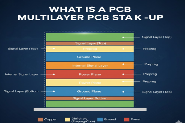
When I talk about stack-ups, I'm thinking about the complete picture: material types, layer thicknesses, and copper weights. This design is critical for achieving signal integrity, managing electromagnetic interference (EMI)[^6], and distributing power efficiently. My factory insights reveal that a good stack-up balances electrical needs with manufacturing feasibility.
Understanding the Core Elements
- Copper Layers: These are the conductive paths for signals and power.
- Dielectric Layers: Insulating materials separating the copper layers.
- Core: A rigid, pre-cured fiberglass epoxy laminate.
- Prepreg: A fiberglass cloth impregnated with epoxy resin, which softens and flows during lamination.
| Element | Description | Function |
|---|---|---|
| Signal | Carries high-speed data. | Transmits data with minimal distortion. |
| Power | Provides stable voltage to components. | Ensures reliable power delivery. |
| Ground | Reference for signals, dissipates heat. | Reduces noise, provides heat dissipation. |
| Dielectric | Insulating material (core/prepreg) between layers. | Maintains electrical isolation. |
| Via | Conductive path connecting different layers. | Allows inter-layer connections. |
What are the different layers present in a circuit board?
Do you know what each layer in your PCB does? Understanding their roles is key to design success. Each layer has a specific job, from carrying signals to providing power and ground.
In a multilayer PCB, different types of layers work together to create a functional circuit board. These typically include signal layers for data transmission, power planes for consistent voltage, and ground planes for noise reduction and heat dissipation.
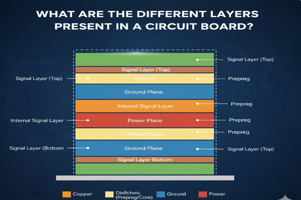
I've seen many designs where engineers overlook the importance of each layer's function, leading to unexpected issues. My experience taught me that properly segmenting and isolating these layers is crucial. For instance, putting a ground plane next to a high-speed signal layer provides a clear return path, reducing EMI. This understanding comes from countless hours spent troubleshooting and optimizing designs in my factory.
Common Layer Types
- Signal Layers: These layers are dedicated to routing traces for signals. They are typically found on the outer layers (top and bottom) and also interleaved within the stack-up for more complex designs.
- Power Planes: Solid copper layers that distribute power to components. They provide a low impedance path for current and help to filter noise.
- Ground Planes: Similar to power planes, these are solid copper layers that serve as a common reference voltage. They are essential for signal integrity, EMI shielding, and heat dissipation.
| Layer Type | Primary Function | Placement Considerations |
|---|---|---|
| Top Layer | Component mounting, initial signal routing. | Often high-density signal, or mixed signal/power. |
| Bottom Layer | Component mounting, final signal routing. | Similar to top, often for lower speed signals. |
| Inner Signal | Complex signal routing, impedance control. | Between power/ground planes for shielding. |
| Power Plane | Stable power distribution. | Adjacent to ground planes for capacitance. |
| Ground Plane | Signal reference, noise reduction, heat sink. | Adjacent to power/signal layers. |
What is the standard board thickness?
Worried about your PCB fitting into its enclosure? Board thickness is critical. Standardizing ensures compatibility and consistent manufacturing processes.
The standard PCB thickness is approximately 0.062 inches (about 1.57 mm), a legacy from the early days of electronics manufacturing using 1/16-inch thick substrates. This dimension is widely adopted for many applications, balancing cost and performance.
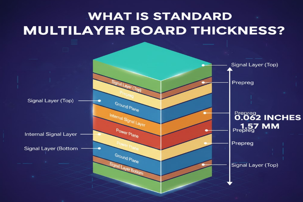
In my work, I often encounter discussions about board thickness. While 0.062 inches is common, I've seen a wide range of requirements. For example, my factory routinely produces ultra-thin boards around 0.2 mm for compact wearables, and ultra-thick multilayer boards exceeding 8 mm for high-power industrial applications. This flexibility is vital, but always consider the mechanical and electrical implications of your chosen thickness.
Factors Influencing Board Thickness
- Mechanical Stability: Thicker boards are more rigid and less prone to warping.
- Electrical Performance: Thickness affects impedance and signal integrity, especially for high-frequency designs.
- Manufacturing Constraints: The number of layers and material choices influence achievable thickness.
| Thickness (mm) | Description | Typical Applications | Notes |
|---|---|---|---|
| 0.2 - 0.8 | Ultra-thin boards | Wearables, smart cards, flexible electronics | Often requires specialized manufacturing processes. |
| 1.0 - 1.2 | Thinner standard boards | Compact consumer electronics, some mobile devices | Balances space-saving with reasonable rigidity. |
| 1.57 (0.062") | Standard thickness | General purpose electronics, industrial controls | Most common, cost-effective, widely supported. |
| 2.0 - 3.2 | Thicker boards | High-power applications, server boards, backplanes | Increased mechanical strength, better heat dissipation. |
| > 3.2 | Ultra-thick boards (>8mm possible) | High-current applications, automotive, aerospace | Custom manufacturing, specialized drilling and lamination required. |
How are multilayer circuit boards made?
Curious about how complex PCBs come to life? Multilayer board manufacturing is a precise process. It combines several layers through meticulous lamination and etching.
Multilayer circuit boards are made by sequentially bonding pre-fabricated core layers with prepreg layers under high temperature and pressure. This process, called lamination, permanently joins the copper and dielectric materials to form a robust, integrated board structure.
From my perspective in the factory, making multilayer PCBs is an art form driven by science. Each step, from etching inner layers to the final lamination, requires immense precision. I've seen how tiny errors in alignment or temperature can compromise an entire batch. That's why quality control at every stage, especially during lamination and drilling, is non-negotiable for my team. It’s about building complexity with consistency.
Key Manufacturing Steps
- Inner Layer Fabrication: Individual core layers are cleaned, imaged, and etched to create the inner circuit patterns[^7].
- Lamination: Multiple etched core layers are interleaved with prepreg sheets. This stack is then subjected to heat and pressure, causing the prepreg to flow and cure, bonding all layers together.
- Drilling: After lamination, holes (vias) are drilled through the entire stack to connect different layers.
- Outer Layer Fabrication: The outer layers are then plated with copper, imaged, and etched to form the final traces and pads.
- Plating and Finishing: Via walls are plated with copper, and surface finishes[^8] (e.g., HASL, ENIG) are applied.
| Process Step | Description | Purpose |
|---|---|---|
| Inner Layer Etching | Photoresist applied, exposed, developed, and copper is etched. | Defines the circuit patterns on individual core layers. |
| Stacking & Lamination | Cores and prepreg stacked, then pressed and heated. | Bonds all layers into a single, monolithic PCB. |
| Drilling | Mechanical or laser drilling of holes through the laminated stack. | Creates vias for inter-layer connections and component mounting. |
| Desmear/Deburr | Chemical cleaning to remove resin residue from drilled holes. | Ensures good adhesion for subsequent copper plating inside the vias. |
| Electroless Copper | Thin layer of copper deposited on hole walls. | Makes the non-conductive hole walls conductive for electrolytic plating. |
| Outer Layer Imaging | Photoresist applied, exposed, developed for outer layer patterns. | Defines the final circuit patterns on the top and bottom layers. |
| Electrolytic Plating | Thick layer of copper and tin/lead plated onto outer layers/vias. | Builds up trace thickness and reinforces via conductivity. |
| Final Etching | Tin/lead resist removed, exposed copper etched away. | Creates the final traces and pads on the outer layers. |
| Solder Mask Application | Green or colored protective layer applied and cured. | Protects traces, prevents solder bridging, insulates. |
| Surface Finish | ENIG, HASL, OSP applied to exposed copper pads. | Prevents oxidation, improves solderability. |
Conclusion
Building a multilayer PCB stack-up[^2] is crucial for robust electronic design. Understanding each layer's role, standard thicknesses, and manufacturing processes ensures optimal performance.
[^1]: Understanding PCB signal integrity is essential for ensuring reliable electronic performance and minimizing issues. [^2]: Learn the intricacies of multilayer PCB stack-up design to enhance your circuit's performance and reliability. [^3]: Discover the importance of dielectric materials in maintaining electrical isolation and performance. [^4]: Gain insights into how prepreg contributes to the structural integrity of multilayer PCBs. [^5]: Understanding the core's function is vital for designing robust and effective multilayer PCBs. [^6]: Learn how to manage EMI in PCB design to enhance performance and reliability. [^7]: Understanding circuit pattern creation is essential for effective PCB design and functionality. [^8]: Explore various surface finishes to improve solderability and protect PCB components.

