

Struggling with unreliable circuit boards? I faced constant signal interference[^1] in my early designs. Multilayer PCBs solved this by adding internal layers. Start planning your stack-up immediately.
I design multilayer PCBs[^2] by first planning the layer stackup[^3], placing components strategically, and using inner layers for stable power/ground connections. Then I carefully route signals across outer and inner layers while ensuring proper via placement. Always perform simulations and follow DFM rules for reliable results that manufacturers can build.
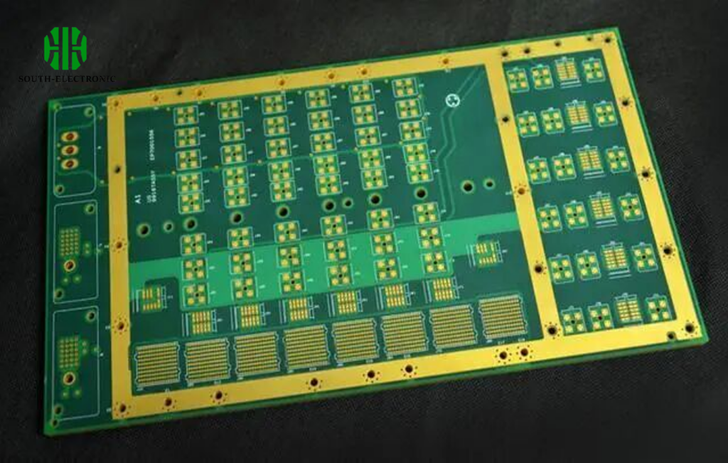
My approach evolved from costly prototyping mistakes. Understanding core principles prevents signal issues and manufacturing headaches in multilayer applications. The following sections share hard-earned workflow optimizations that solve real-world problems.
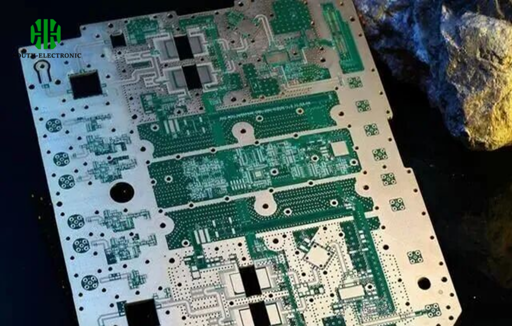
What Materials Are Best for High-Frequency Multilayer PCBs?
Signal loss plagues high-frequency circuits. Wrong materials create multilayer pcb application nightmares. Low-Df substrates preserve signal strength.
Rogers RO4000 series and PTFE composites perform best for high-frequency multilayer PCBs. Their ultra-low dissipation factors maintain signal integrity above 1GHz. Avoid standard FR4 since its inconsistency causes dielectric losses that cripple microwave/RF designs.
Critical Material Properties and Alternatives
High-frequency demands focus beyond conductivity. Three key properties determine success:
- Dielectric Loss Control: Df values under 0.004 prevent energy absorption
- Thermal Stability: Z-axis CTE matching prevents delamination
- Moisture Resistance: 24GHz | Near-flat curve | 15× FR4 |
| FR4/Hybrid | Below 500MHz | Poor stability | Low cost |
For 5G multilayer pcbs, I combine RO4350B cores with Isola’s low-loss prepreg. This balances cost versus performance when creating 12-layer cellular baseband units. Humidity tests matter—submerge samples for 48 hours before acceptance as part of your multilayer pcb manufacturing process.
How to Avoid Common Manufacturing Defects in Multilayer PCBs?
Ever opened stacked inner layers to find voids? Lamination defects crash your project. Prevention starts at design phase.
Avoid defects by maintaining copper balance across layers, verifying drill-to-copper clearances, and specifying exact impedance tolerances to the fab. Use tear-drop pads and matched thermal relief patterns to prevent solder voids and thermal stress fractures during assembly.
Top Failure Points During Multilayer PCB Manufacturing Process
Process deviations cause 78% of multilayer failures. Three critical failure types require distinct tactics:
-
Delamination Solutions
Balance copper distribution (±10% across layers)
Specify Tg>170°C materials for lead-free assembly
Pre-bake laminates before pressing -
Drilling Damage Prevention
Maintain 0.15mm hole-to-copper clearance
Use stepped laser vias in HDI designs
Implement via-in-pad fill processes
| Defect | Cause | Prevention Cost |
|---|---|---|
| Pad Cratering | CTE mismatch | $0.02/pad reinforcement |
| Acid Traps | Acute routing angles | $150 DFM review fee |
| Barrel Cracks | Thin plating | $300 panel-level testing |
My worst multilayer pcb example involved $2K lost to micro-cracks. Now I mandate cross-section reports for first articles. Temperature cycle testing from -40°C to 125°C exposes weaknesses before mass production. Always confirm material certificates match purchase specifications.
What factors affect Multilayer PCBs cost?
Unnecessary layers drain budgets fast. Over-specification cripples product margins in high-volume multilayer pcb applications.
Material selections drive 50% of expense according to data from my industrial clients. Balancing layer count against performance achieves 30% savings versus initial quotations.
Major Cost Drivers and Budget Strategies
| Cost Factor | Influence Level | Optimization Tactic |
|---|---|---|
| Layer Count | ★★★★★ | Reduce by 2 layers via via-in-pad |
| Material Grade | ★★★★☆ | Hybrid stackups: FR4 core + high-speed prepreg |
| Special Features | ★★★☆☆ | Limit gold plating to edge connectors |
| Tolerances | ★★★★☆ | Only critical nets need ±5% impedance |
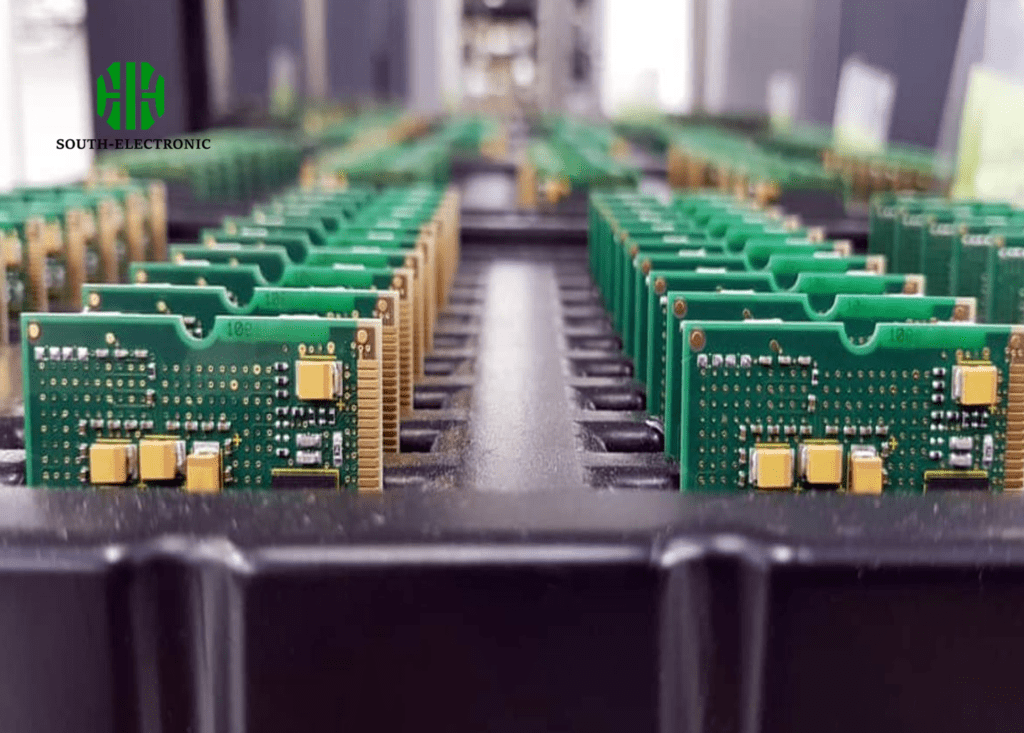
High-reliability military multilayer pcbs demand specialized materials like Arlon di-clad 88i. For commercial IoT products I combine FR4 with partial Rogers sheets which avoids multi layer board wood costs. Blind via quantity spikes expenses – replace staggered microvias with straight laser drills where possible. Prototype with low-cost manufacturers first.
Conclusion
Thoughtful stackup planning prevents signal and thermal issues in multilayer pcbs. Match materials to your frequency needs and implement strict manufacturing feedback loops to control costs while avoiding defects.
[^1]: Understand the sources of signal interference and how to mitigate them in your designs.
[^2]: Explore the advantages of multilayer PCBs for improved signal integrity and design flexibility.
[^3]: Learn effective strategies for planning layer stackups to enhance PCB performance.

